SoC voltages everywhere!! AMD’s terror! To find out more about this issue, we have to go back to the source, which is no other but SVI3. In this article I will try to shed more light into this power interface used by AMD’s newest processors.
After posting the article and especially after the video, many users complained that I didn’t measure behind the CPU’s socket and that there could be a substantial voltage drop on the PCB traces. Since I know that the corresponding traces are thick enough to NOT allow for high voltage drops, and from the fact the VRMs have current sense lines to adjust their output according to the load and voltage drops, I wasn’t so worried about that. Nonetheless, I took new measurements on the mainboard’s measurement pads and behind the CPU’s socket.
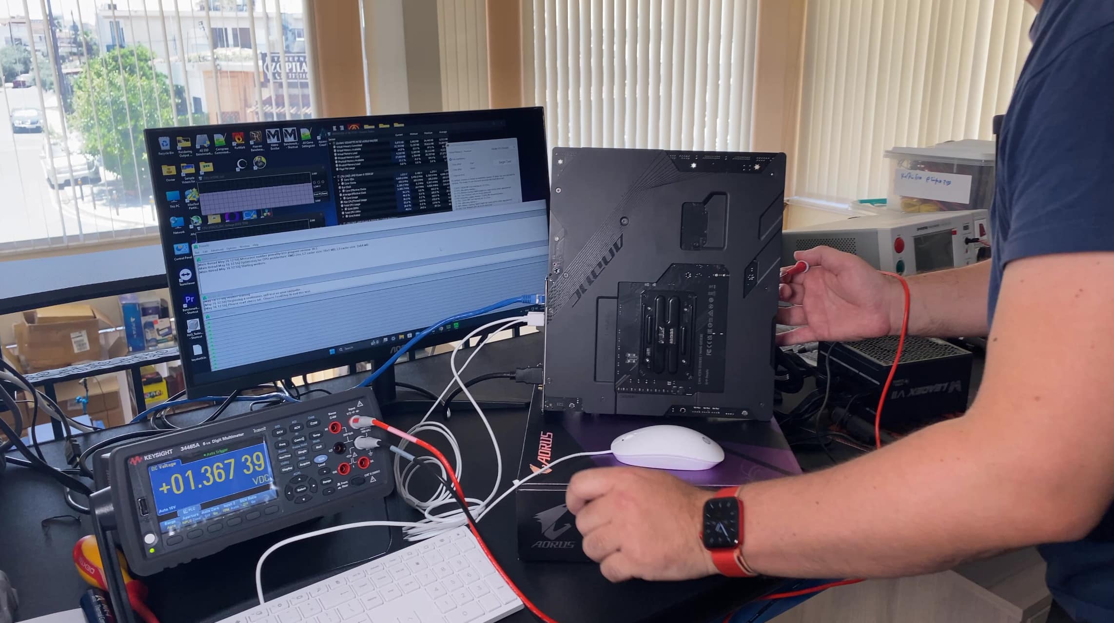
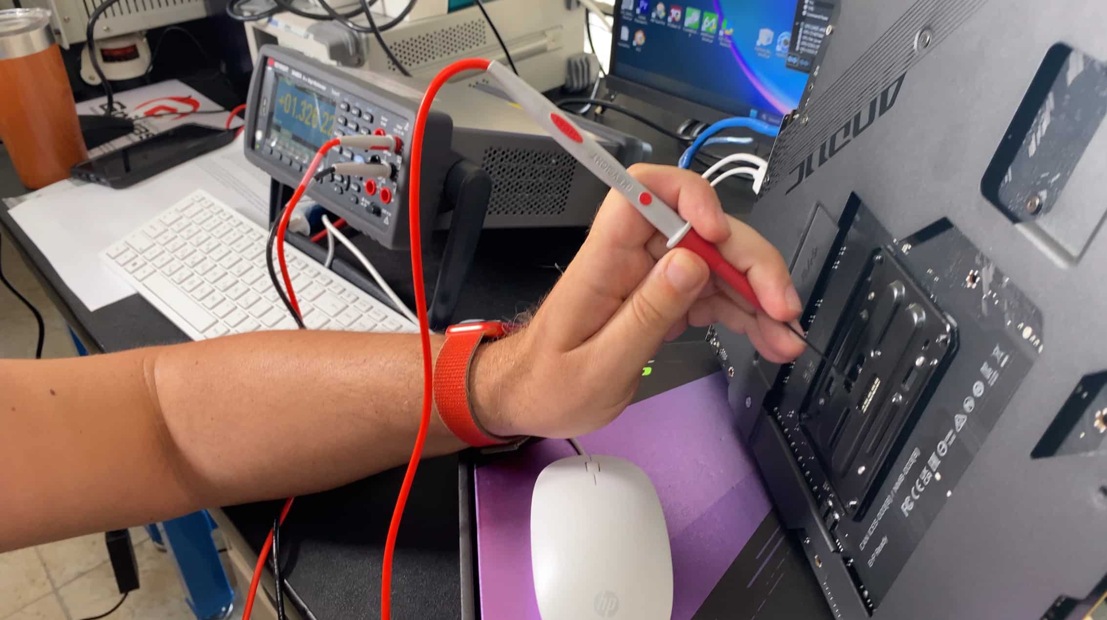
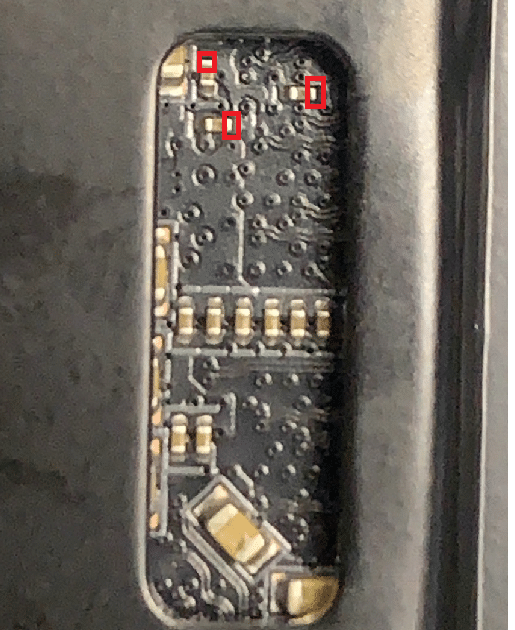
As you can see, the drop between the mainboard’s VRM output and the socket is just 0.01445V, with Prime95 running, stressing the CPU to the max. Since we settled this, let’s proceed with the main article, which concerns SVI3.
Scalable Voltage Interface 3 (SVI3)
SVI3 is designed to allow faster and more precise control over the voltage required from the processor. It establishes a two-way communications protocol between the CPU and the mainboard’s voltage regulator modules (VRMs), allowing the CPU to control its power requirements besides monitoring power input. There are some PWM controllers which are compatible with the SVI3 interface. The CPU has real-time information on the mainboard’s VRM performance and operating conditions. When the CPU doesn’t need much power, it can shut down some VRMs to lower energy losses.

The CPU can enable or disable the power phases of the VRMs by sending, through the I2C bus, the corresponding command to the power controller.
The AM5 socket has three different power rails through which the CPU is powered. One is shared between the CPU and embedded graphics cores; the SoC rail is mainly for the I/O Die (IOD), and the VDD rail is for the Infinity Fabric and other miscellaneous stuff.
There is almost no information about SVI3 from AMD. This is why I had to search the older SVI2, where SVI3 is based. Modern CPUs must dynamically monitor and adjust the voltage rails that feed them accordingly. Since the CPU creates the load, it is ideal to be able to control its power source. This is something that could also be the case in power supplies. Actually, the ATX v3.0 and PCIe 5.0 standards through the 12VHPWR connector and its sense signals: CARD_PWR_STABLE and CARD_CBL_PRES# (Optional) which, however, are optional, and I don’t see them implemented eventually.
Back to the topic at hand, the SVI2 and SVI3 are three-wire interfaces with clock (SVC), data (SVD), and telemetry (SVT) lines. The SVI2 and SVI3 protocols are similar to the I²C bus concept, so the CPU is the master sending control packets through the SVC (clock) and SVD (data) lines to the mainboard’s VRM circuits.
In SVI2, the control packets consist of 3 bytes transmitted conforming to the SMBus send byte protocol: 1 byte for selecting the voltage domain (Core or SOC) followed by an acknowledgment (ACK) bit, and then 2 bytes containing the voltage to be applied and other configuration parameters, each byte followed by an ACK bit. Due to the configuration encoding, the voltage can be configured with a step size of 6.25 mV. Through the telemetry function (TFN) configuration bits, periodic voltage (and current) reports from the VR to the CPU via the SVC and SVT lines can be enabled.
In SVI3, we have three rails, Core, SoC, and VDD, so in the control packet, the first byte has to be used for three options instead of two in SVI2. The VRMs of the mainboard receive or transmit I2C signals using the I2C interface. The CPU sends various commands (Read/Write/Reset registers, VID/Address packets, Change Power State, and Telemetry Request) to the VRMs. There is a loop control, which controls the power-on/off sequence of the VRMs, handles protection features, and controls the PWM operation of the VRMs.
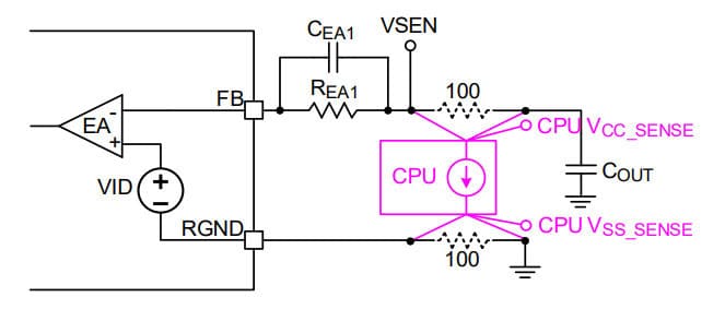
The CPU contains on-die sense pins, VCC_SENSE and VSS_SENSE. If no CPU is installed and the vendors want to test the mainboard, the pair of 100Ω resistors are required to close the circuit and provide output voltage feedback. VSEN and RGND must be routed as differential pairs from the VRM controller to the CPU socket without crossing any phase node, gate driver, VIN power delivery path, and high-speed signals. The VSEN is ideal for taking accurate measurements without considering voltage drops.
The most important is that there is a remote sense line between the VRMs and the load (the CPU) to handle the voltage drops along the PCB traces, the CPU’s internal power routers, and socket contacts. So there is not only a voltage drop on the mainboard’s PCB, but we also have a drop at the mainboard’s pins that connect to the CPU and within the CPU!
For telemetry information, the CPU takes data from the controller, which continuously monitors the output voltage of the VRMs, from the differential voltage sense input (VSEN pin and RGND pin). Some power controllers average the data for higher accuracy to reduce measurement noise. The controller also senses current output information (Iout) and temperature information to the CPU. So if the CPU finds that something is wrong, through the provided data, it can make the corresponding changes to the VRM operation.
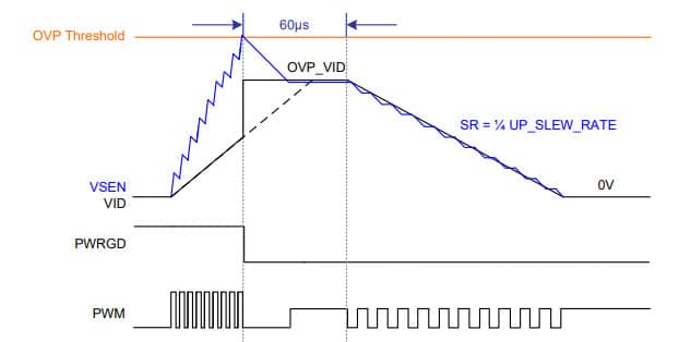
I want to state that most protection features are handled by the mainboard’s power controller, including overcurrent, over-temperature, undervoltage, and overvoltage protection. For example, when OVP is triggered, the controller forces the low-side MOSFETs to turn on, so the high-side MOSFETs will turn off, and the VRMs will be disconnected from the PSU’s input (12V).
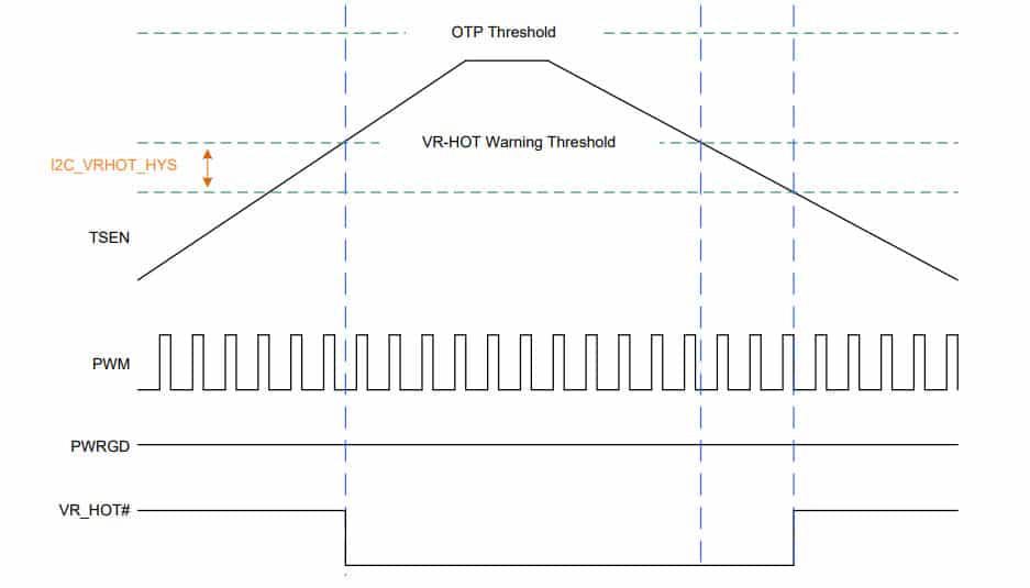
Regarding overtemperature protection, when the controller receives an “overheat” signal, it transmits it to the CPU through the I2C bus, and it drops power consumption by reducing the CPU’s load. This is why the quality of the VRMs matters for the CPU’s speed. If VRMs get quickly hot during overstress, the CPU has to drop its load to allow them to cool down.
Conclusions
From all the above, we can come to the following conclusions
- SVI3 allows the CPU to control the mainboard’s VRM phases fully.
- The SVI3 can get but also provide all kinds of measurements, including, of course, all voltage levels fed to the CPU’s corresponding circuits.
- The only way to get voltage readings within the CPU is by utilizing SVI3.
- We cannot know if the readings that SVI3 provides within the CPU are accurate since we cannot measure them externally.
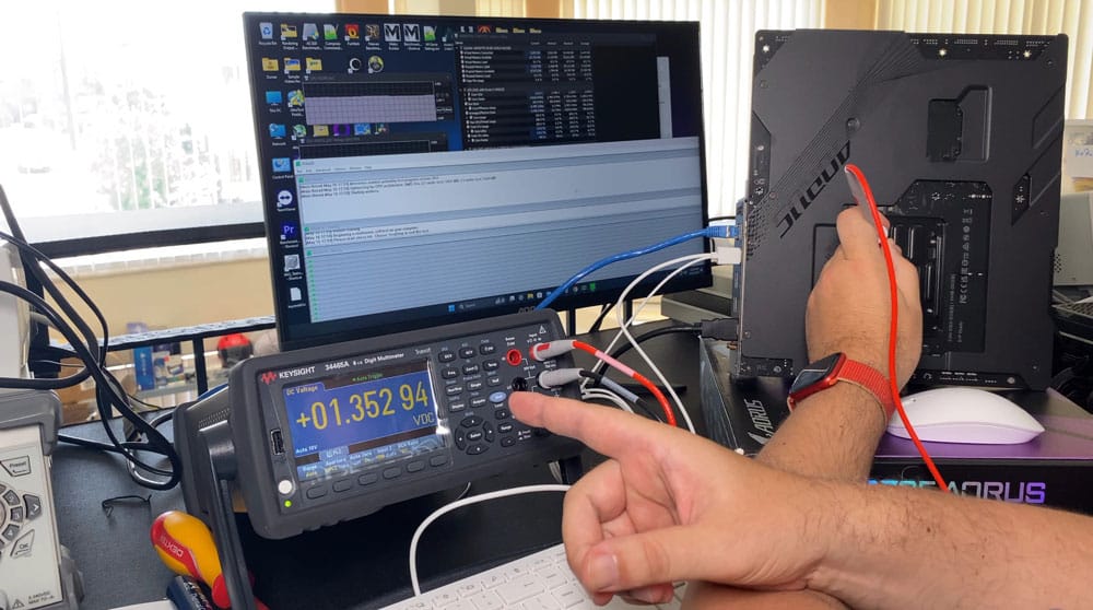
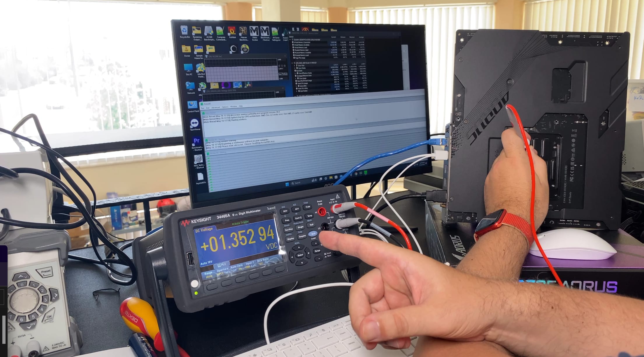
- There is a voltage drop between the mainboard’s VRM output and the socket, which in my case, for the VSOC, under a full load, is 0.01445V.
- There is a voltage drop between the socket’s power input and what the CPU’s internal circuits get because of the connections through the mainboard’s pins and the power losses within the CPU’s internal power traces. In my case, I measured 1.35294V at the back of the socket, while the CPU VDDCR_SOC (SVI3 TFN) Voltage, as reported by HWinfo, was 1.295V. This means that from behind the socket and up to the CPU’s corresponding circuit, the voltage drop is 0.05794V, while if you take the mainboard’s VRM output as the start point, the voltage drop is 0.07239V, which is substantial.
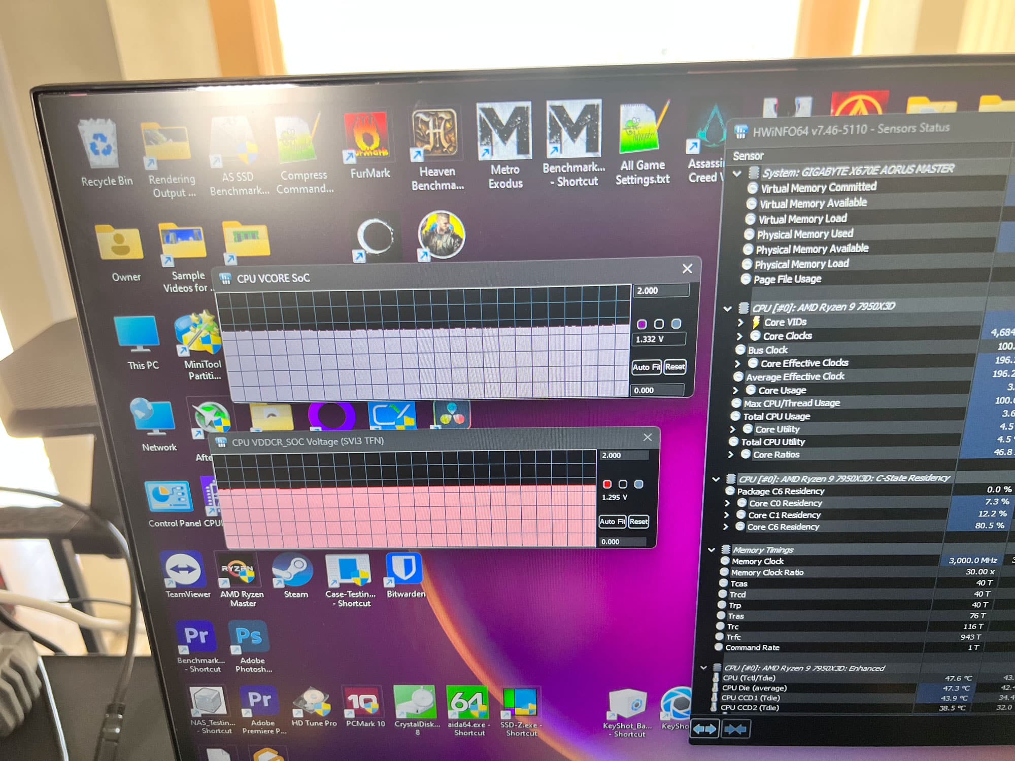
AMD has declared that anything above 1.30V VSOC is unsafe and should be avoided, but it didn’t clarify at which point. On the VRMs of the mainboard, at the back of the socket, or the CPU’s internal circuit? I had some talks with Gigabyte’s people, and they told me that they try to keep the VSOC voltage below 1.3V according to the SVI3’s information, meaning at the CPU’s internals, where we cannot take readings through any physical means, but only through software. Any lower VSOC SVI3 voltage than 1.30V, for example, 1.25V, creates problems for RAM kits with the EXPO profile enabled.
From all the above, I can safely assume that if you check your mainboard CPU VDDCR_SOC Voltage (SVI3 TFN) and find it below 1.30V while running a stressful benchmark and with EXPO enabled, you are safe, always according to AMD. For me, it is a problem that I cannot take physical measurements of this voltage, and I am troubled by the significant voltage drop of 0.05794V between the CPU socket and the circuit within the CPU.
References
- Advanced Micro Devices, Inc. 2018. Understanding Power Management and Processor Performance Determinism. Retrieved 2023-05-17 from https://www.amd.com/system/files/documents/understanding-power-management.pdf
- Buhren, R., Jacob, H. N., Krachenfels, T., & Seifert, J. (2021). One Glitch to Rule Them All: Fault Injection Attacks Against AMD’s Secure Encrypted Virtualization. ArXiv. /abs/2108.04575
- Renesas Electronics Corporation. 2020. ISL62776 Multiphase PWM Regulator for AMD CPUs Using SVI2. Retrieved 2023-05-17 from https://www.renesas.com/us/en/document/dst/isl62776-datasheet
- Richtek Technology Corporation. 2023. Dual Channel PWM Controller with I2C Interface Control for
AMD SVI3 CPU/GPU Core Power Supply. Retrieved 2023-05-17 from https://www.richtek.com/assets/product_file/RT3667BT/DS3667BT-00.pdf
Here is a list of affiliate links to get some good PSUs to use with Powenetics and/or your AMD system:
Did AMD previously gave any statement regarding safe SoC values for Ryzen 5000 processors? For example my Gigabyte B450 motherboard sets the voltage at 1.2v auto while XMP 3600MHz profile on a 5800X3D is enabled. SVI2 readings show values ranging from 1.1875v to 1.20v in idle and under load, under load it mostly stays on 1.2v. When I contacted Gigabyte support they simply said that as long as it is stable there is nothing to be worried about.
I didn’t follow AMD on this I am afraid but as far as I know there weren’t any issues with the 5000 series regarding SoC.