Part Analysis
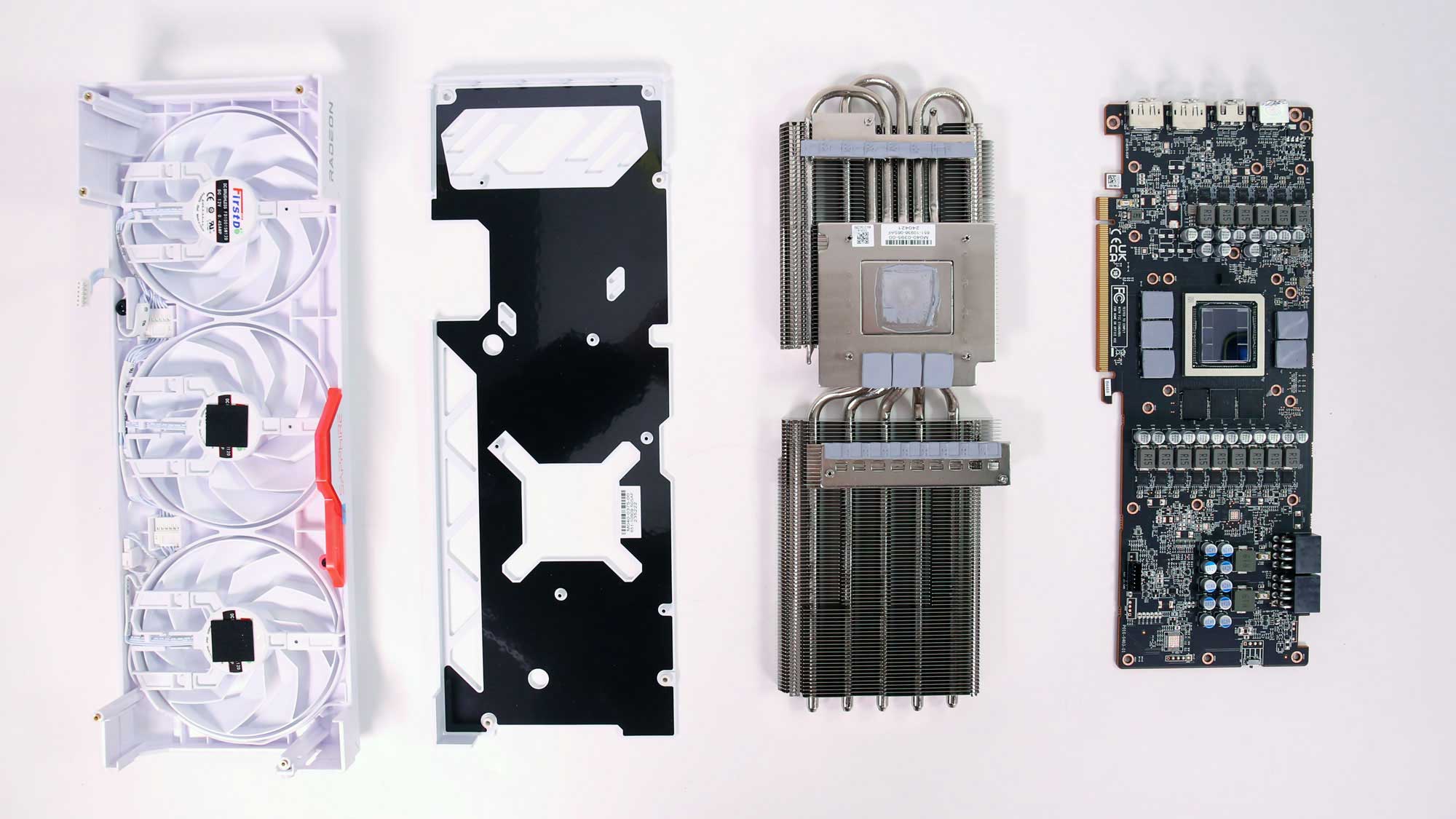
Breaking apart graphics cards is fairly easy, much easier compared to PSUs or mobile phones and laptops.
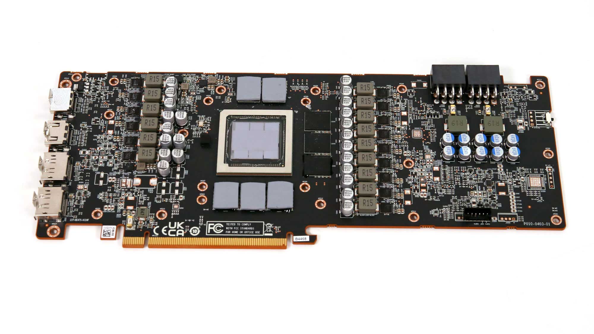
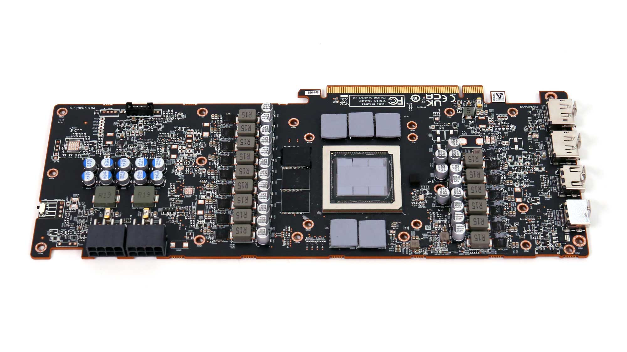
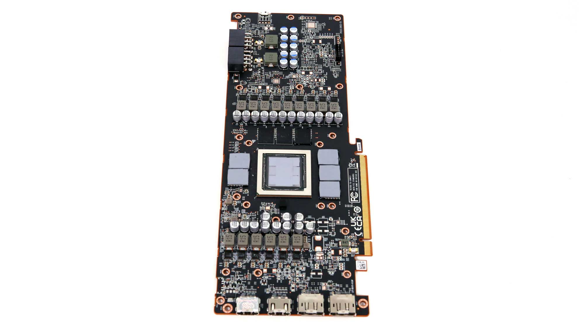
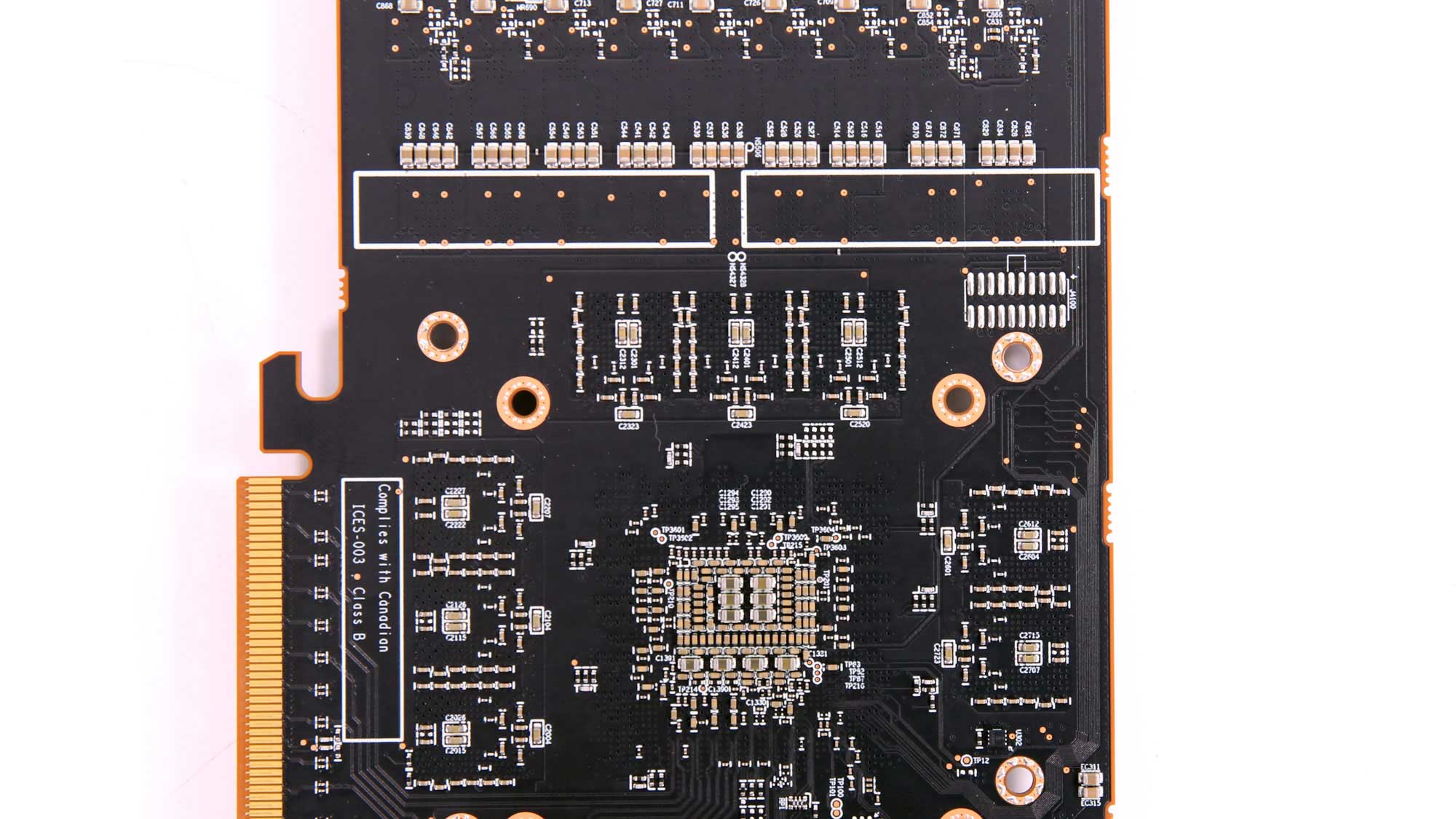
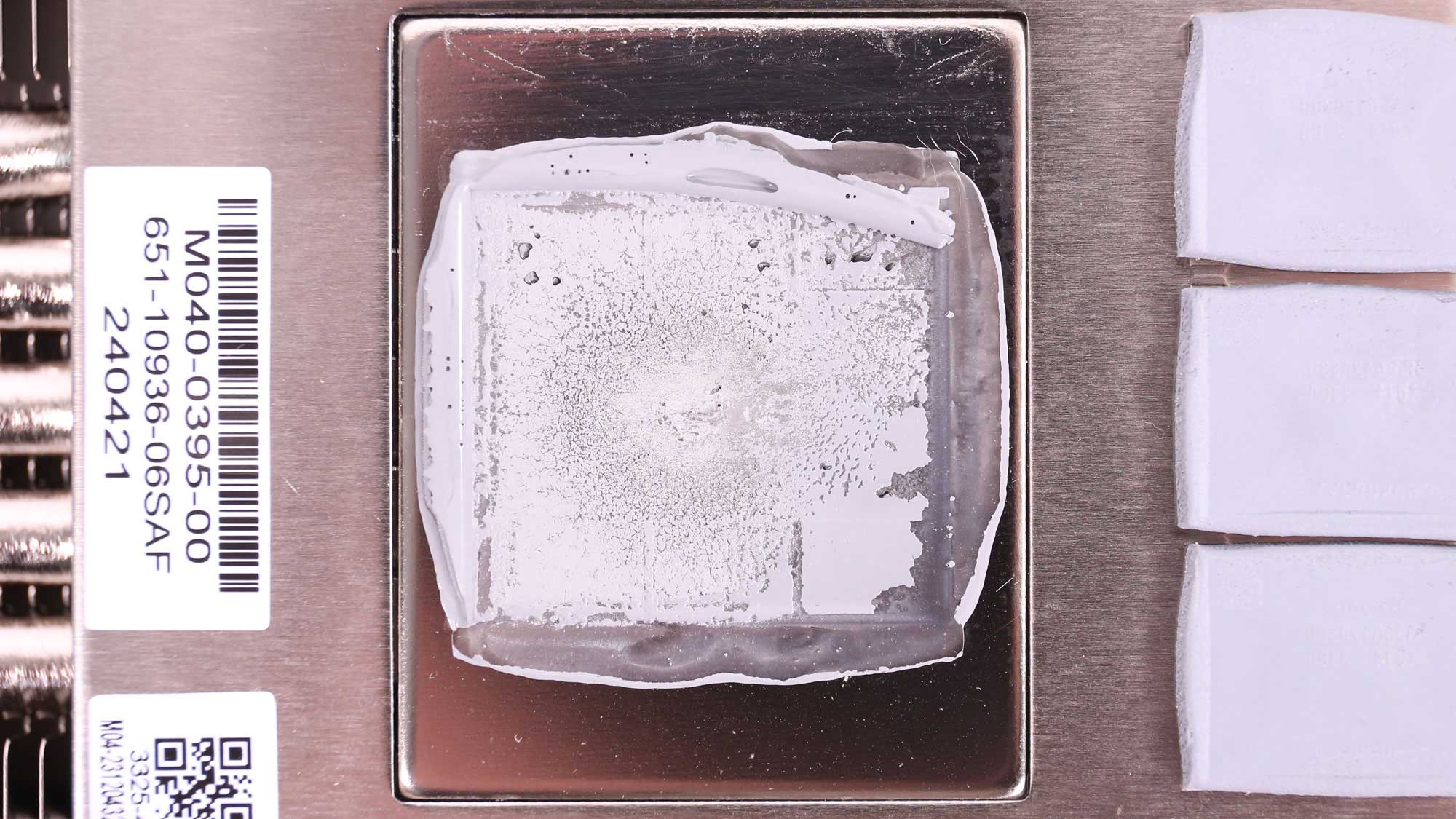
Photos of the PCB’s front side. I expected a white PCB!
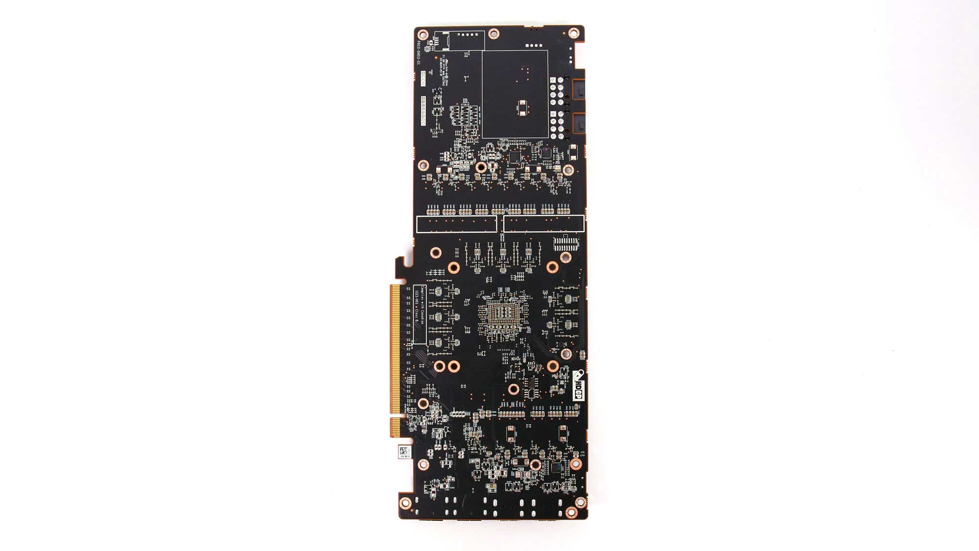
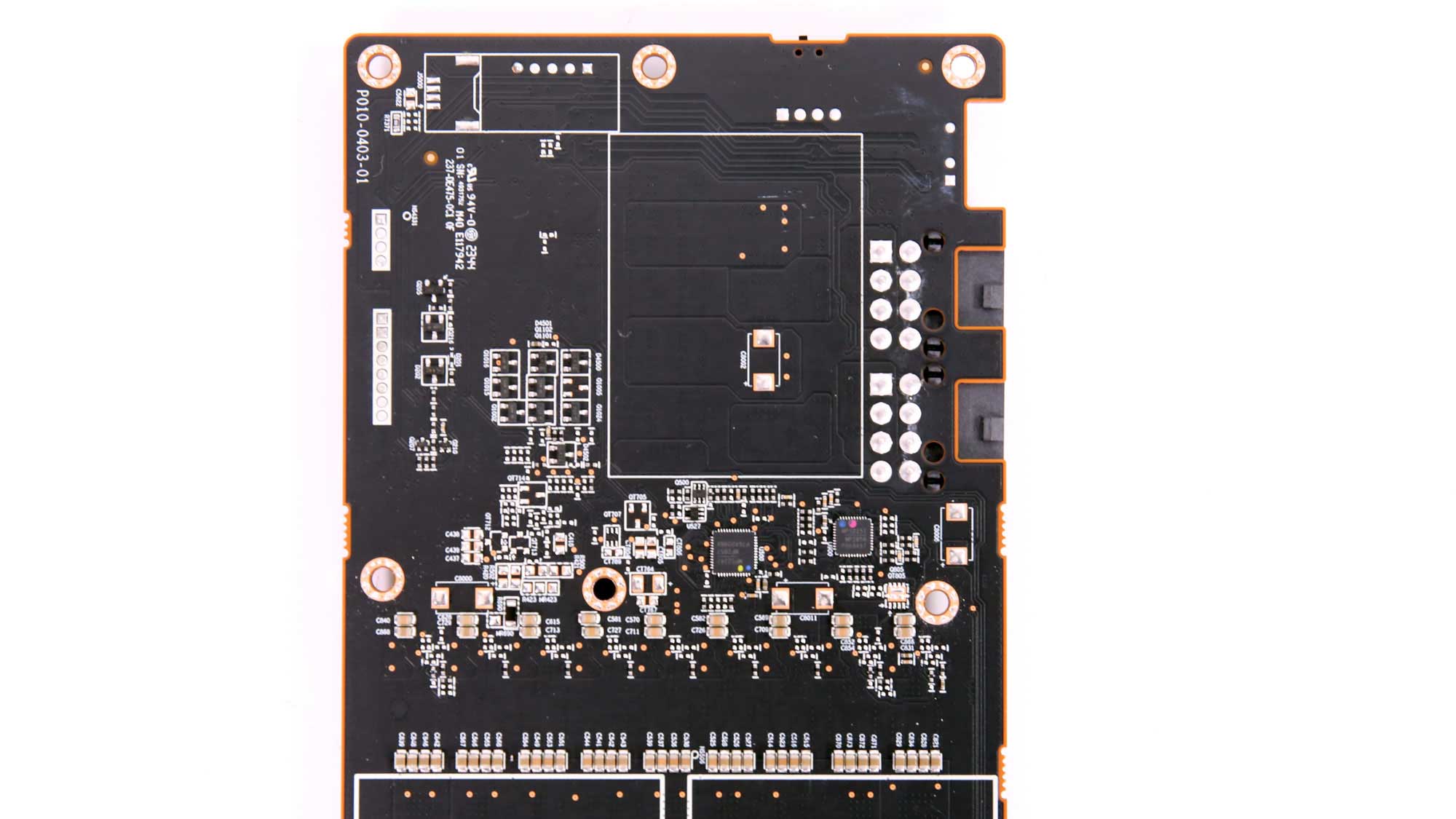
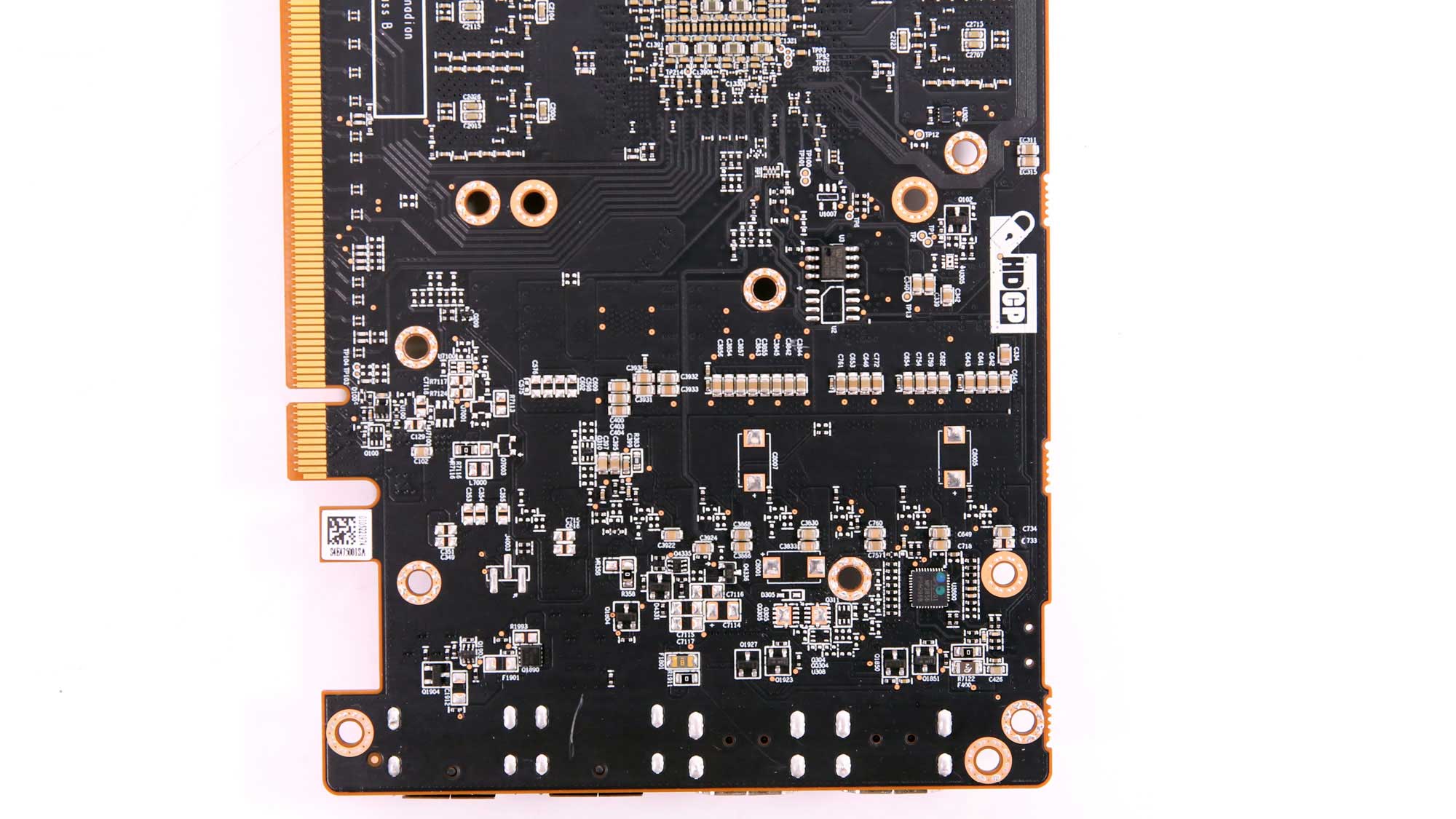
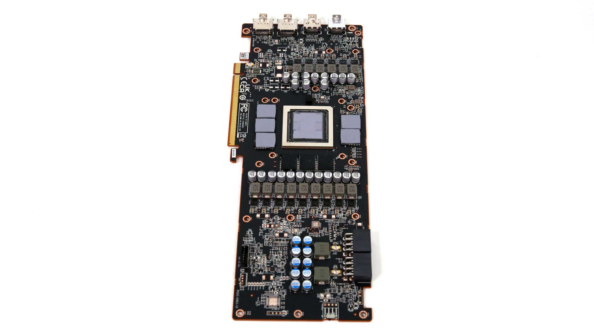
Photos of the PCB’s backside.
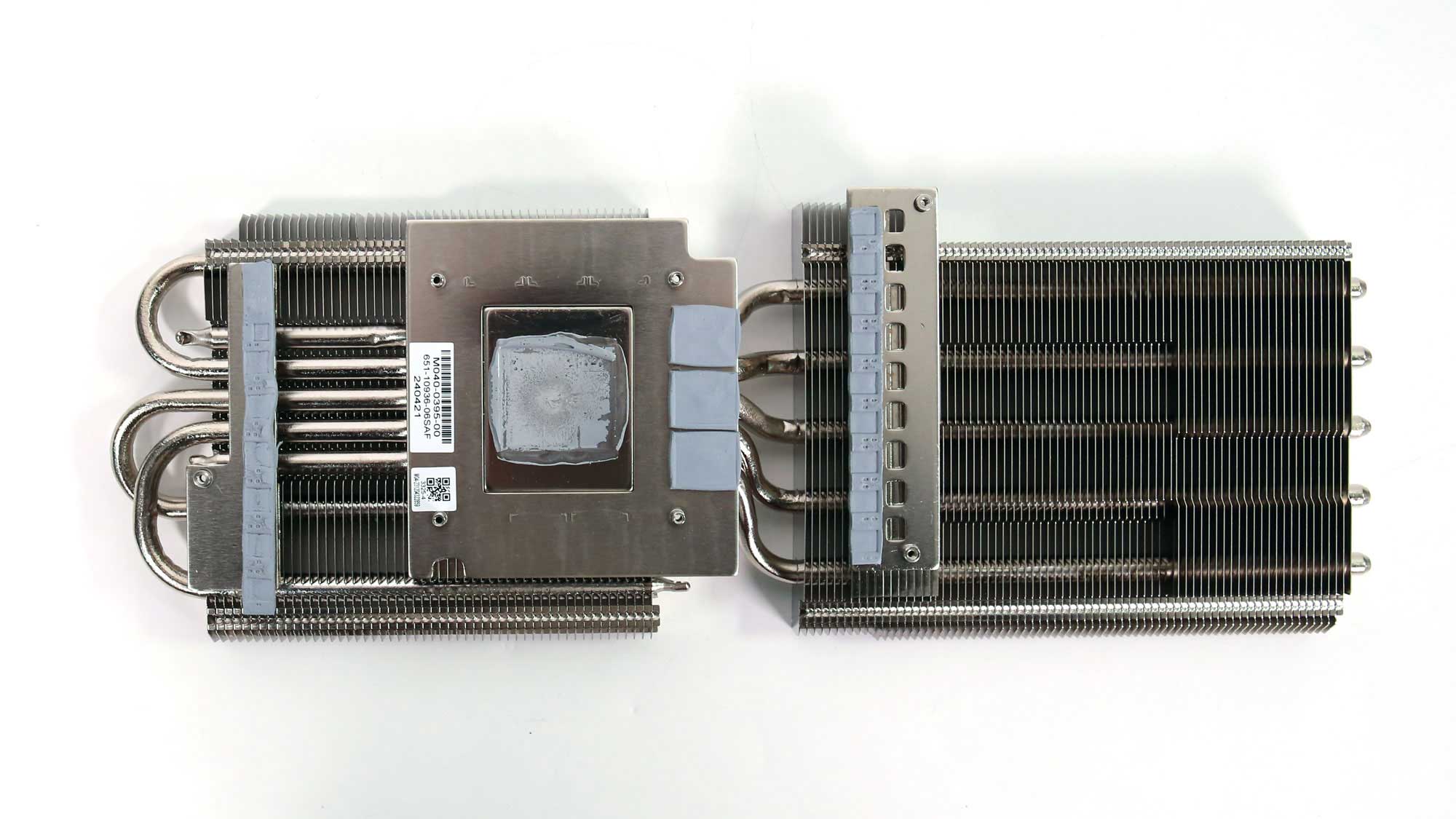
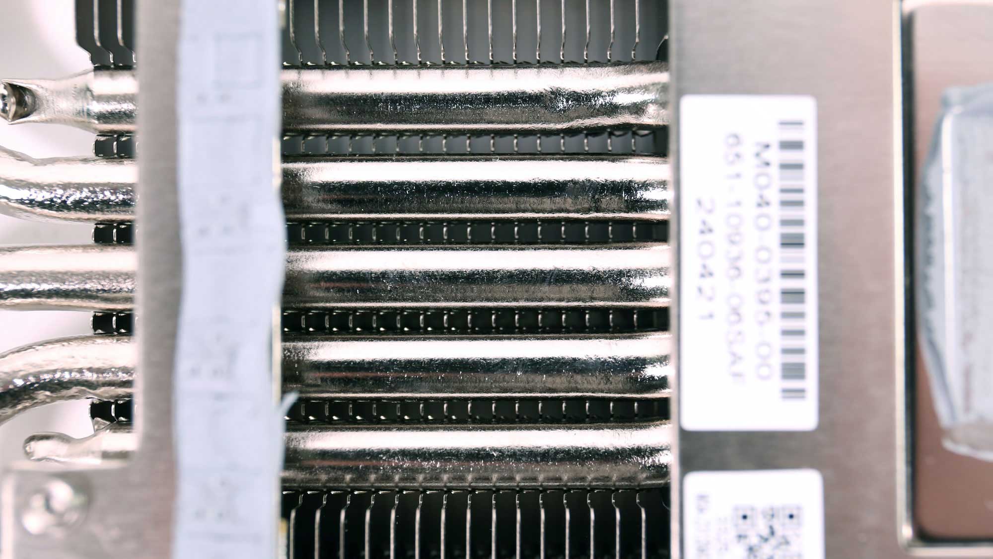
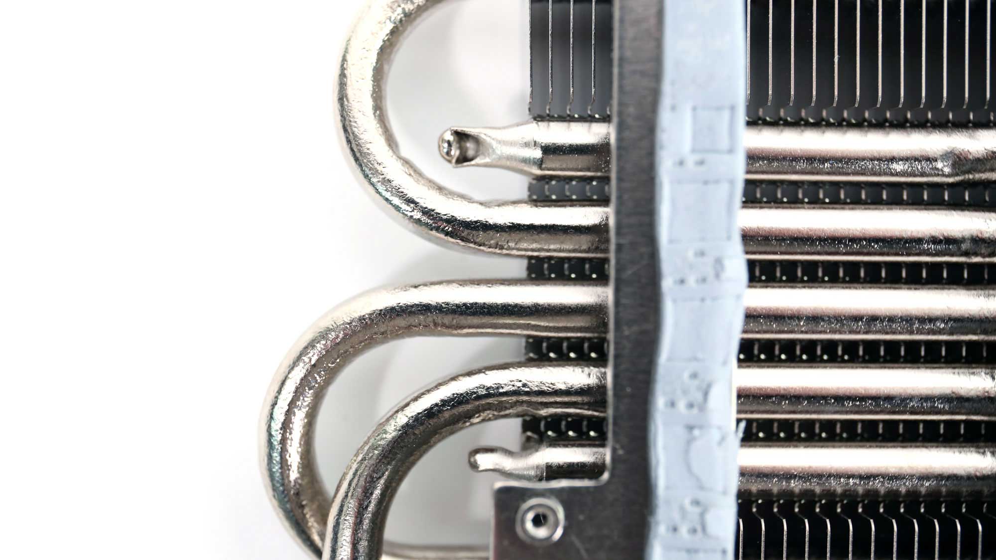
The cooling solution is large enough to handle the GPU’s 250W TDP easily.
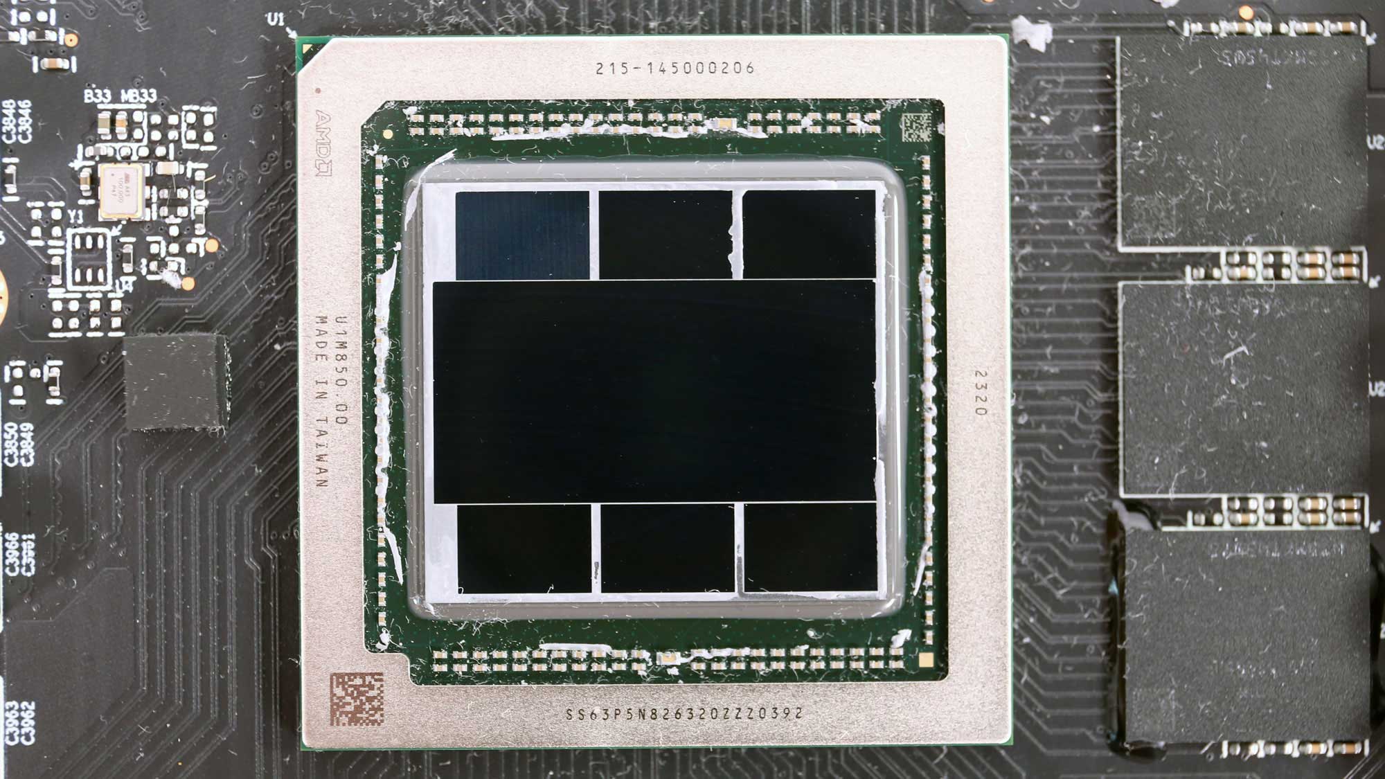
The Navi 31 GPU. The full-size graphics compute die is surrounded by six memory cache dies, but only four are real! The other two are dummies to ensure the cooling solution’s optimal contact under pressure. The GCD uses TSMC’s 5 nanometer node manufacturing technology and has a die size of 300mm2, while the MCDs are made with TSMC’s 6 nanometer manufacturing, and their die size is 36.6 mm2 each.
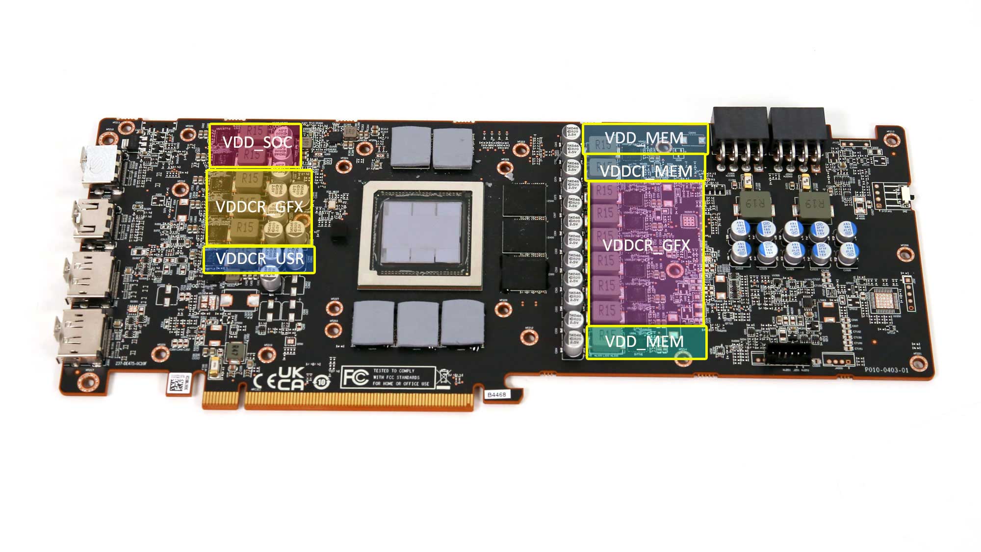
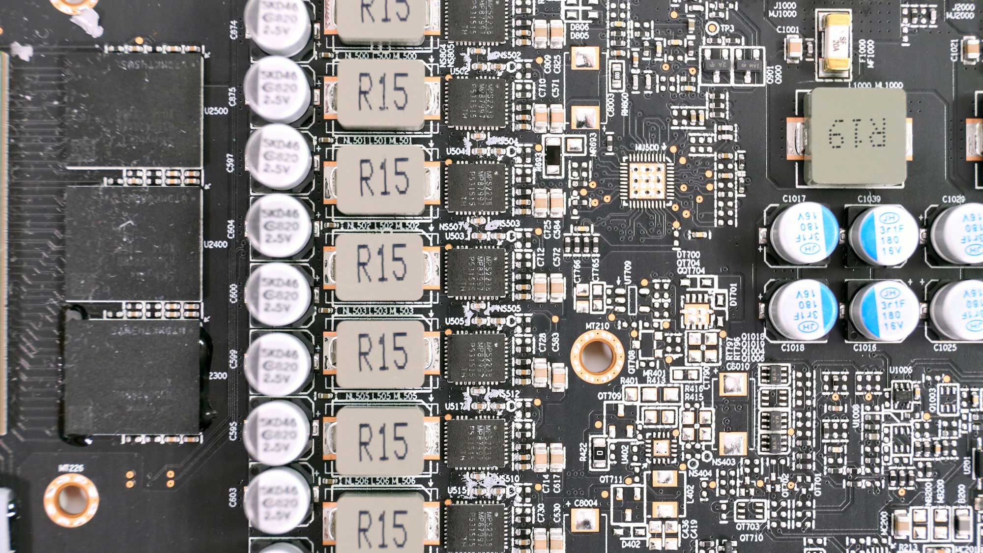
I only managed to do the scheme above thanks to my friend Igor’s help since I am not yet highly familiar with GPU design. But I will get there soon! The VDDCR_GFX uses nine power phases, controlled by a MP2857 IC. Two plus one phases handle VRAM.
 |
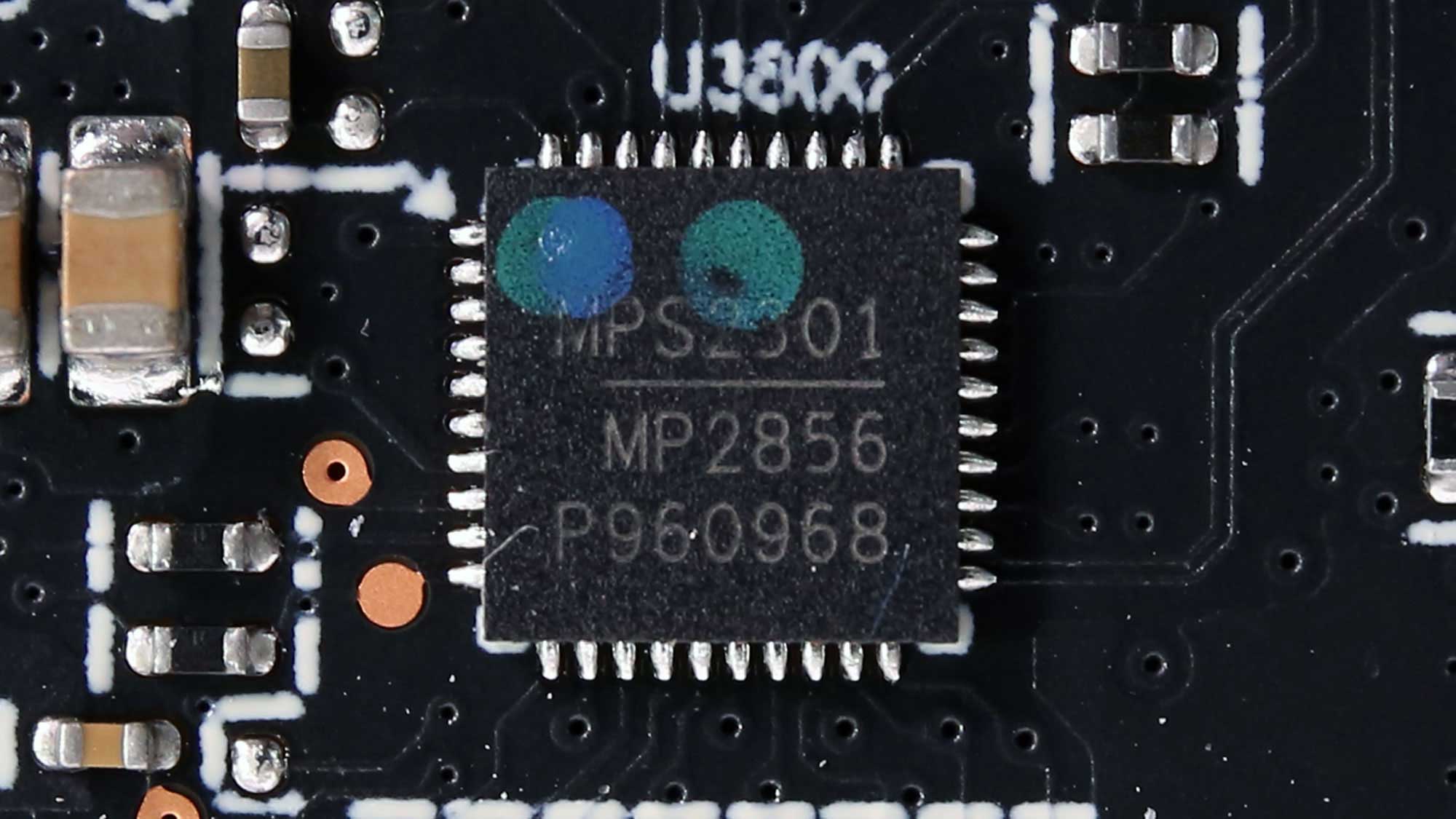 |
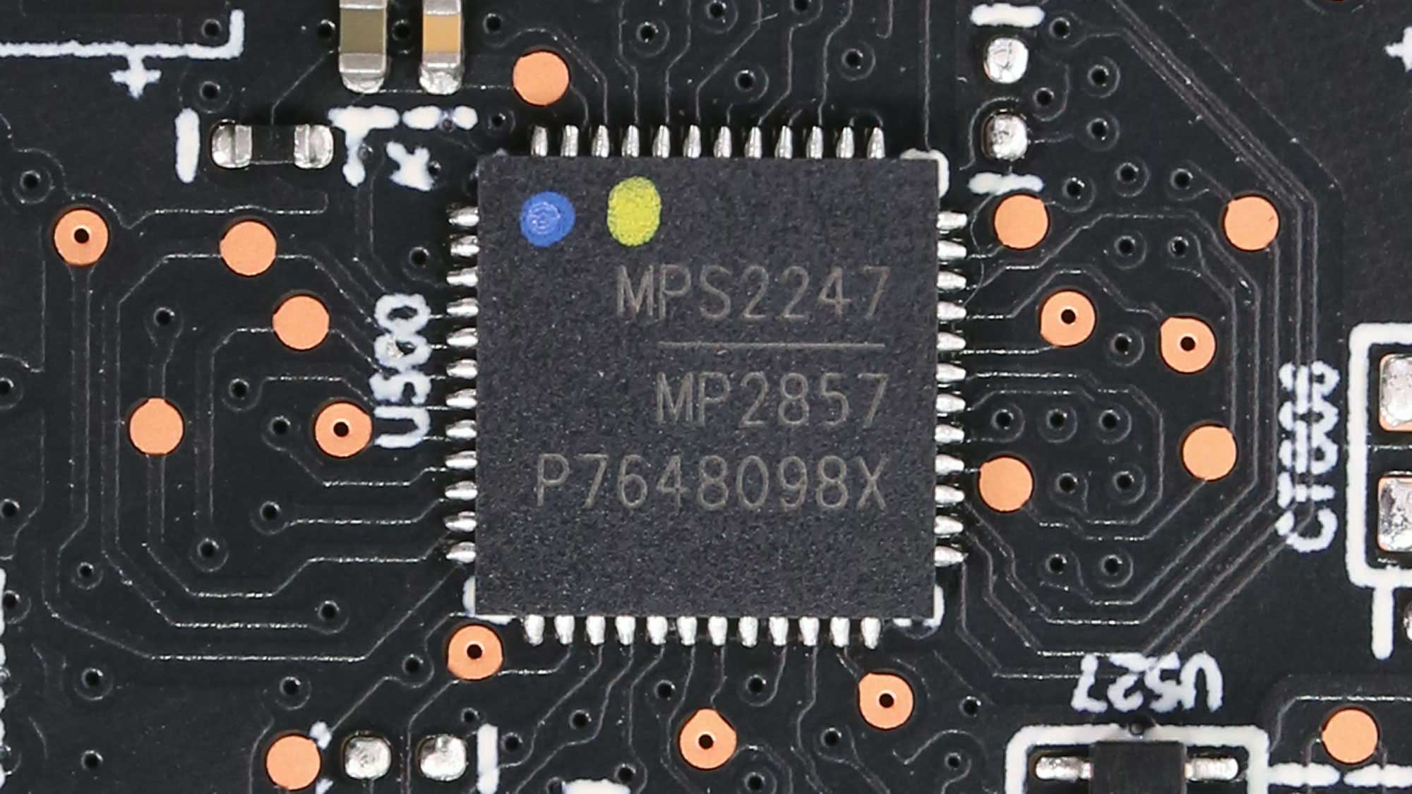
The card’s PWM controllers, a single Monolithic Power Systems MP2857 and two MP2856.
 |
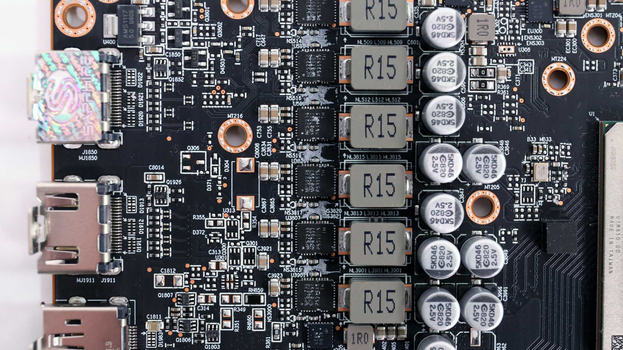 |
The GPU’s VRMs use Monolithic MP87997 DrMOS components, rated for 70A max each. The same DrMOS are used by the VRAM phases.
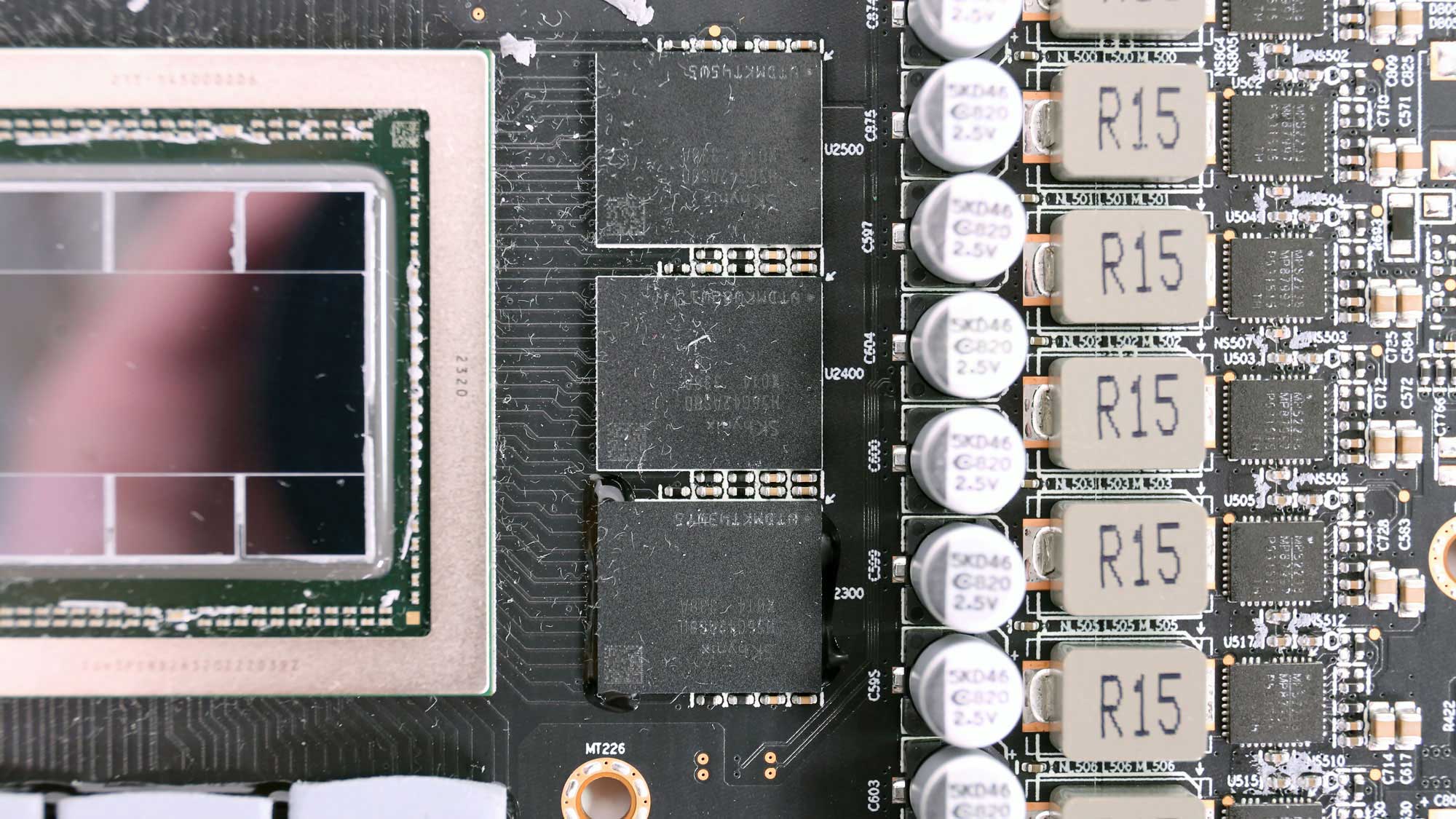
Hynix makes the GDDR6 memory chips, and their model number is H56G42AS8DX-014. They are rated at 2500 MHz (20 Gbps effective).
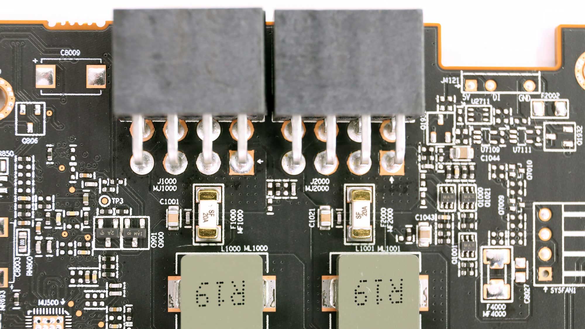
The card’s dual PCIe 6+2 pin sockets. Right below them are two 20A SMD fuses, meaning that the incoming power in each connector is expected to be below 240W (given 12V nominal voltage). For very short periods, power spikes, these fuses won’t be blown and I found that hard way, since I measured spikes exceeding 500W.
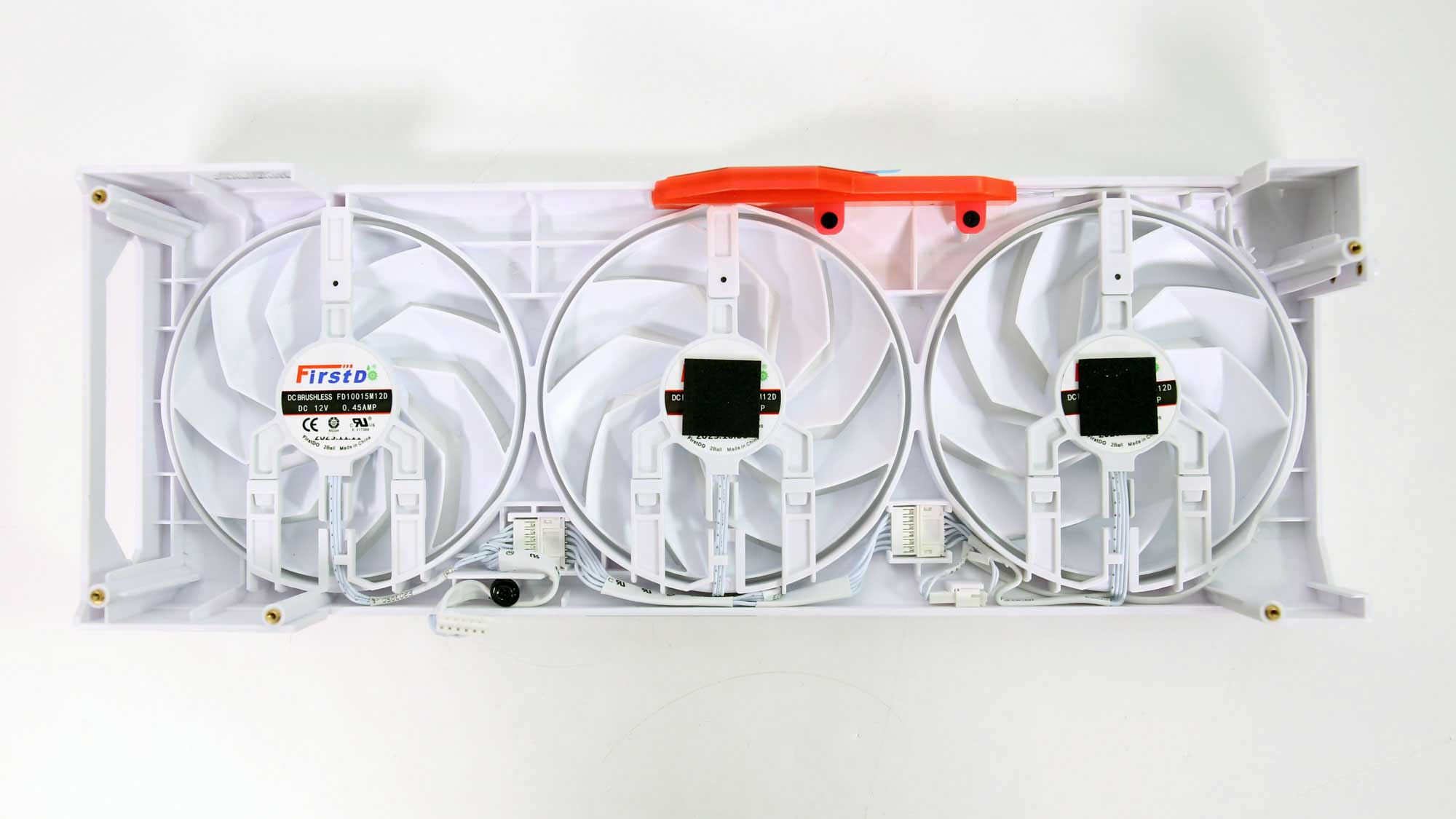
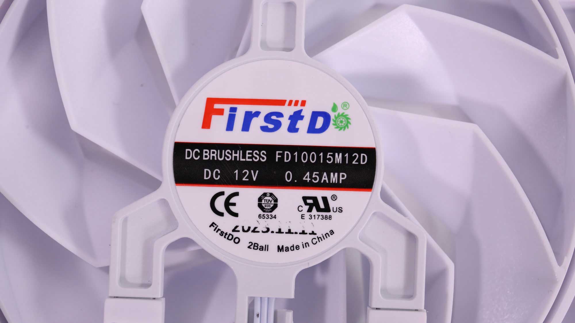
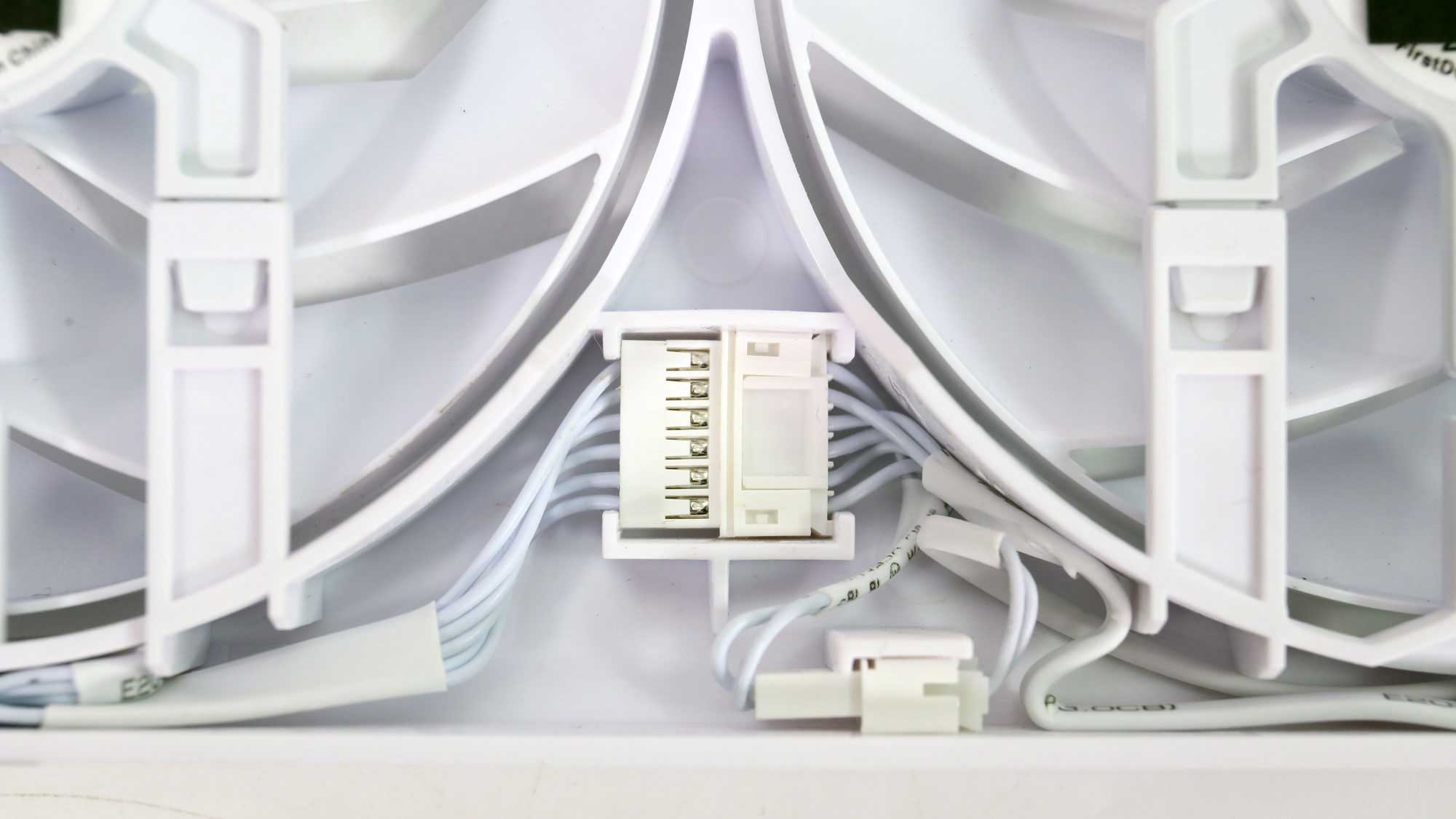
This is the first time I have seen this fan brand. The model number is FD10015M12D, and their diameter is rather unusual, at 95mm.
- Prologue & Technical specifications
- AMD’s Key Technologies
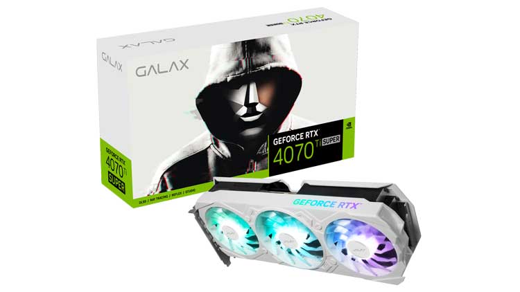
- Box & Contents
- Part Analysis
- Specifications Comparison
- Test System
- Game Benchmark Details
- Raster Performance
- RT Performance
- RT Performance + DLSS/FSR Balanced
- Raytracing Performance + DLSS/FSR Balanced + FG
- DLSS/FSR Balanced (No RT)
- DLSS/FSR Balanced + FG (No RT)
- Relative Perf & Perf Per Watt (Raster)
- Relative Perf & Perf Per Watt (Raster + DLSS/FSR)
- Relative Perf & Perf Per Watt (RT)
- Relative Perf & Perf Per Watt (RT + DLSS/FSR)
- Relative Perf & Perf Per Watt (RT + DLSS/FSR + FG)
- Rendering Performance
- Operating Temperatures
- Operating Noise & Frequency Analysis
- Power Consumption
- Clock Speeds & Overclocking
- Cooling Performance
- Epilogue