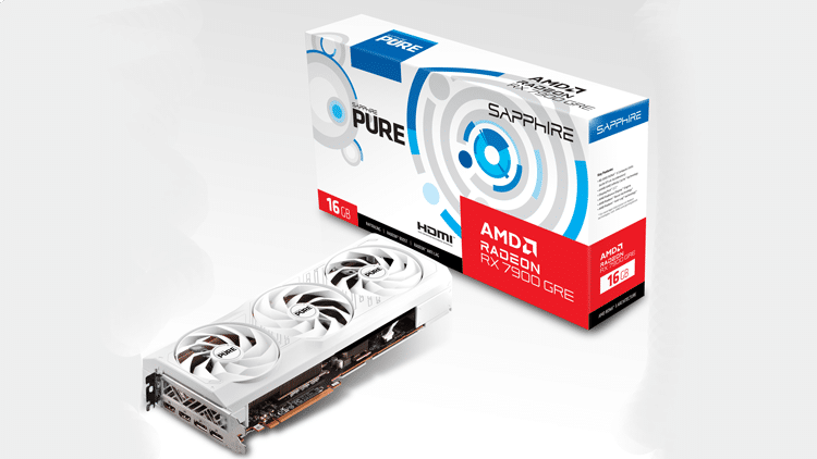
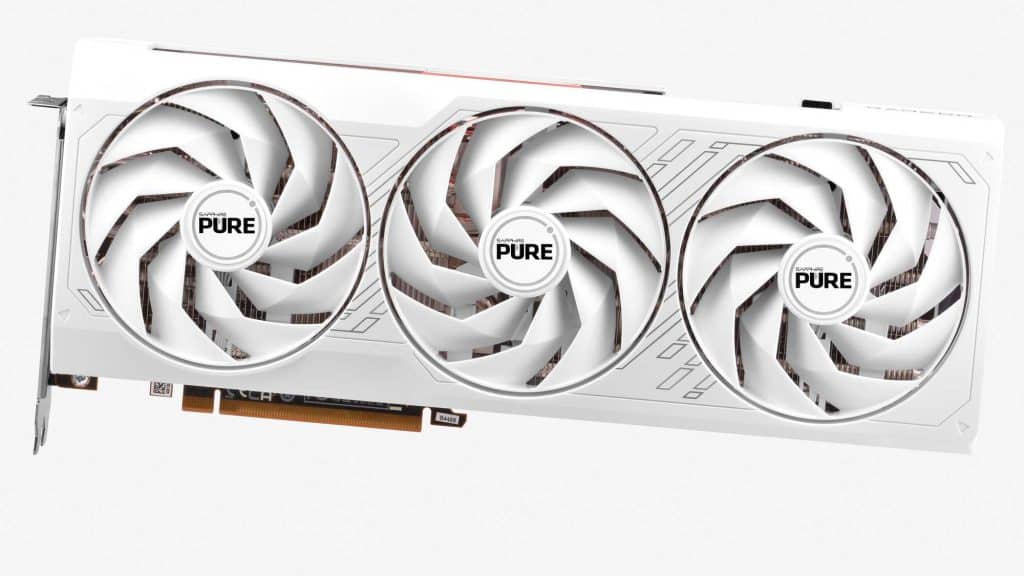
The Sapphire Radeon RX 7900 GRE uses a GPU that is not new, since it was launched in July 2023 in China. AMD decided to ship it worldwide now, at a starting price of $550 to cope with NVIDIA’s RTX 4070, whose price was recently cut, with the introduction of the RTX 4070 Super.
The fun part of the RX 7900 GRE is that it is not a new product since it was launched in the Chinese market last year. AMD decided to offer it worldwide because of the price cut in the NVIDIA RTX 4070 once its super variant was launched. It uses a variant of AMD’s Navi 31 GPU, which uses the RDNA 3 architecture, and its starting price is 550 dollars, addressing the mid-gaming section.
- AMD Radeon RX 7800 XT & RX 7700 XT Performance, Power Analysis & Noise Output
- Galax GeForce RTX 4070 Ti Super EX Gamer White Performance, Power Analysis & Noise Output
Compared to the RX 7800 XT, the 7900 GRE has the same VRAM and about $50 increased price, but it also has more computing units (CUs), 80 vs 60, and more ROPs. It uses a cost-effective version of the high-end Navi 31 GPU, which only supports 256-bit memory interface bandwidth; this is why the card comes with 16 GB of VRAM. The TDP is also lower at 260W. Compared to the line flagship, the RX 7900 XTX, the RX 7900 GRE has 80 CUs instead of 90 and 160 ROPs instead of 192. Moreover, the Infinity Cache size is half. Compared to the 7900 XT, the GRU variant has fewer CUs (80 instead of 84), fewer ROPs (160 vs. 192), and shorter memory bandwidth (256-bit vs. 320-bit). Its Infinity Cache is also smaller (64 MB vs. 80 MB).
The RX 7900 GRE focuses mostly in strong 1440p gaming performance, and in some not so demanding titles you can even increase the resolution to 4K.
For more details about the differences between all GPUs mentioned above, and not only, check the following tables.
AMD Graphics Cards Major Specs
| RX 7900 XTX | RX 7900 XT | RX 7900 GRE | Sapphire Radeon RX 7900 GRE | RX 7800 XT | RX 7700 XT | |
|---|---|---|---|---|---|---|
| Architecture | Navi 31 | Navi 31 | Navi 31 | Navi 31 | Navi 32 | Navi 32 |
| Process Technology | TSMC N5/N6 | TSMC N5/N6 | TSMC N5/N6 | TSMC N5/N6 | TSMC N5/N6 | TSMC N5/N6 |
| Base Clock (MHz) | 1929 | 1387 | 1880 | 1972 | 1295 | 1435 |
| Boost Clock (MHz) | 2498 | 2394 | 2245 | 2333 | 2430 | 2544 |
| VRAM Size (GB) | 24 | 20 | 16 | 16 | 16 | 12 |
| VRAM Type | GDDR6 | GDDR6 | GDDR6 | GDDR6 | GDDR6 | GDDR6 |
| VRAM Speed (Gbps) | 20 | 20 | 18 | 18 | 19.5 | 18 |
| VRAM Bus Width (bit) | 384 | 320 | 256 | 256 | 256 | 192 |
| Transistors (Billions) | 57.7 | 57.7 | 57.7 | 57.7 | 28.1 | 28.1 |
| Shading Units | 6144 | 5376 | 5120 | 5120 | 3840 | 3456 |
| TMUs | 384 | 336 | 320 | 320 | 240 | 216 |
| ROPs | 192 | 192 | 160 | 160 | 96 | 96 |
| Compute Units | 96 | 84 | 80 | 80 | 60 | 54 |
| Ray Tracing Cores | 96 | 84 | 80 | 80 | 60 | 54 |
| TDP (W) | 355 | 300 | 250 | 250 | 263 | 245 |
| Launch Month/Year | 11/22 | 11/22 | 7/23 | 2/24 | 8/23 | 8/23 |
| Street Price ($) | 930 | 750 | 550 | 570 | 500 | 420 |
NVIDIA Graphics Cards Major Specs
| RTX 4090 | RTX 4080 Super | RTX 4070 Ti Super | RTX 4070 Super | RTX 4070 | |
|---|---|---|---|---|---|
| Architecture | AD102 | AD103 | AD103 | AD104 | AD104 |
| Process Technology | TSMC 5N | TSMC 4N | TSMC 4N | TSMC 4N | TSMC 4N |
| Base Clock (MHz) | 2235 | 2295 | 2340 | 1980 | 1920 |
| Boost Clock (MHz) | 2520 | 2550 | 2610 | 2475 | 2475 |
| VRAM Size (GB) | 24 | 16 | 16 | 12 | 12 |
| VRAM Type | GDDR6X | GDDR6X | GDDR6X | GDDR6X | GDDR6X |
| VRAM Speed (Gbps) | 21 | 23 | 21 | 21 | 21 |
| VRAM Bus Width (bit) | 384 | 256 | 256 | 192 | 192 |
| Transistors (Billions) | 76.3 | 45.9 | 45.9 | 35.8 | 35.8 |
| Shading Units | 16384 | 10240 | 8448 | 7168 | 5888 |
| TMUs | 512 | 320 | 264 | 224 | 184 |
| ROPs | 176 | 112 | 96 | 80 | 64 |
| Compute Units | 128 | 80 | 66 | 56 | 46 |
| Ray Tracing Cores | 128 | 80 | 66 | 56 | 46 |
| TDP (W) | 450 | 320 | 285 | 220 | 200 |
| Launch Month/Year | 9/22 | 1/2024 | 1/24 | 1/24 | 4/23 |
| Street Price ($) | 2000 | 1150 | 840 | 600 | 550 |
- Form Factor: 2.5 slots, ATX
- Shading Units: 5120
- Boost Clock: 2333 MHz
- Memory Speed: 18 Gbps
- VRAM Size: 16 GB
- Memory Interface Width 256-bit GDDR6
- Memory Bandwidth: 576 GB/sec
- PCI-E 4.0
- Fans: 3x 95mm
- Fan bearing: Double-Ball
- Fan Stop: Yes
- Ports: 2x DisplayPort 2.1a, 2x HDMI 2.1a
- Dimensions(without Bracket): 320(L)X 128.75(W)X 52.57 (H)mm
- Weight: 1123g
- Warranty: two years
- MSRP (excluding VAT): $570
- Prologue & Technical specifications
- AMD’s Key Technologies
- Box & Contents
- Part Analysis
- Specifications Comparison
- Test System
- Game Benchmark Details
- Raster Performance
- RT Performance
- RT Performance + DLSS/FSR Balanced
- Raytracing Performance + DLSS/FSR Balanced + FG
- DLSS/FSR Balanced (No RT)
- DLSS/FSR Balanced + FG (No RT)
- Relative Perf & Perf Per Watt (Raster)
- Relative Perf & Perf Per Watt (Raster + DLSS/FSR)
- Relative Perf & Perf Per Watt (RT)
- Relative Perf & Perf Per Watt (RT + DLSS/FSR)
- Relative Perf & Perf Per Watt (RT + DLSS/FSR + FG)
- Rendering Performance
- Operating Temperatures
- Operating Noise & Frequency Analysis
- Power Consumption
- Clock Speeds & Overclocking
- Cooling Performance
- Epilogue


“RT performance stays notably behind NV’s corresponding offerings”
Not in the same price range. Terrible review