Part Analysis
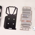
Taking apart the card is easy.
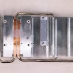
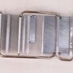
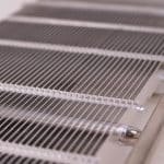
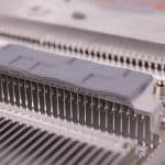
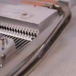
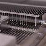
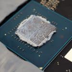
The heatsink with the pair of heatpipes.
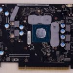
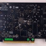
Photos of the PCB’s front and back sides.
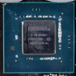
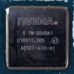
The AD107 GPU. TSMC Taiwan makes it using a 5-nanometer process. It has a die size of 159 mm², enough to host 18.9 billion transistors. You will find more details in TechPoweUp’s GPU database.
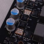
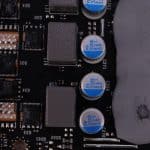
Four power phases provide power to the GPU. A UPI uP9512U controls them. They use UBIQ QN3103 (64A max @ 25C) and QN3107 (68A max @ 25C) FETs for the high and low sides, respectively. A single-phase handles memory using the aforementioned pair of FETs.
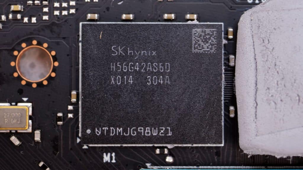
The Hynix GDDR6 RAM chips can do 2250 MHz (18Gbps effective), and their model number is H56G42AS6DX-014.
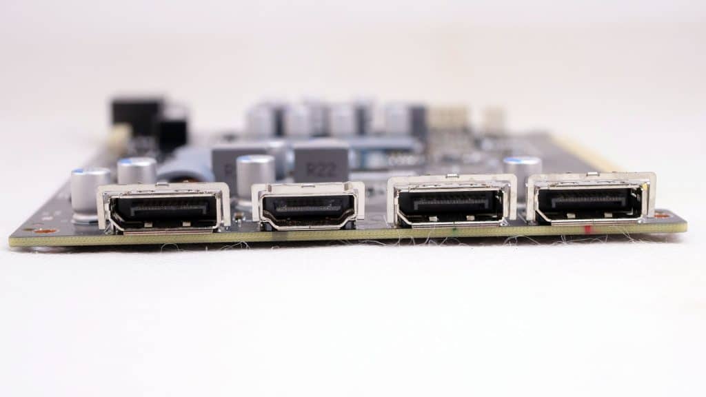
The HDMI and DP ports.
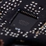
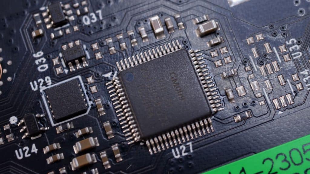
I suspect that this is the RGB controller.
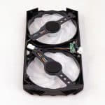
The pair of cooling fans and their frame.
- Metro Exodus
- Red Dead Redemption 2
- Resident Evil Village
- Shadow Of the Tomb Raider
- A Plague Tale Requiem
- Raytracing Performance
- Rendering Performance
- Operating Temperatures
- Operating Noise
- Power Consumption
- Relative Performance
- Performance Per Watt
- Clock Speeds & Overclocking
- Cooling Performance
- Epilogue
