Teardown & Part Analysis
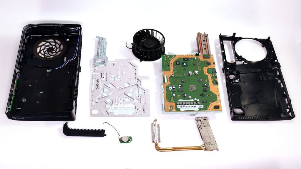
It is not that easy to break apart the PS5 Pro, as is the case for the Slim and previous PS5 models, because of the vast amount of screws that you have to deal with.
Front and rear photos of the PS5 Pro, without the covers.
Some photos of the covers. Removing them isn’t that hard.
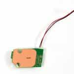
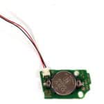
The CMOS battery is much more accessible now in this PS5 Pro, a highly welcome feature for repairmen.
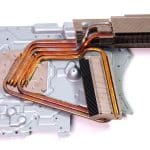
The top cover-heatsink is a huge pain to remove because of the dozens of screws that Sony used (why?)
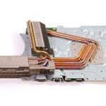
Another smaller heatsink that is held in place only by the thermal paste! I am not sure if this provides optimal cooling.
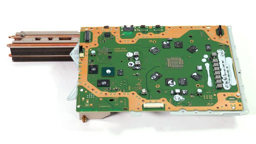
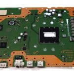
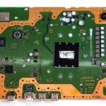
The top side of the mainboard. Still attached to the main heatsink.
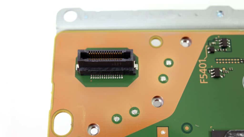
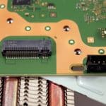
This slot is used to connect the optical drive once Sony makes them available for the PS5 Pro.
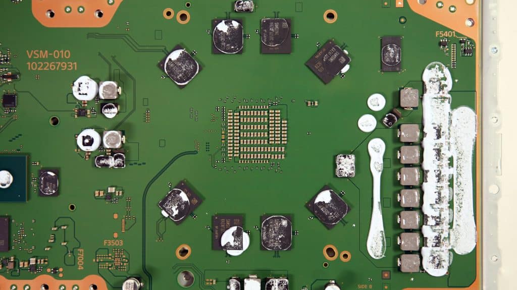
Many capacitors are installed at the back of the APU to help it handle power spikes. The eight large chips surrounding the APU are the GDDR6 RAM modules.
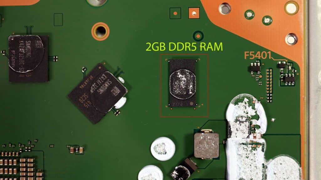
There is an additional DDR5 RAM module (SKhynix -DDR5-5600) in the PS5, which most likely handles the regular OS operations and not the games since it is notably slower than the GDDR6 modules.
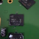
The eight GDDR6 modules are by Samsung (K4ZAF325BC-SC20) and have 2GB capacity each.
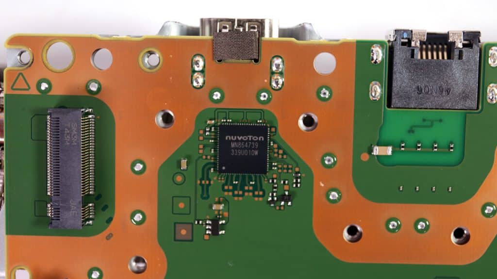
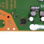
This is the HDMI Encoder IC.
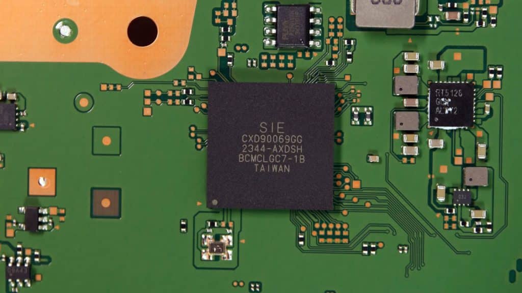
This is the South Bridge, and you should pray not to break because it costs 42 euros!
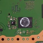
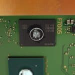
The onboard storage and the storage controller. The Samsung flash memory (K9OUGD8-J1ETCB0) chips are soldered on the mainboard, but you can expand the console’s storage through the mainboard’s NVMe slot. Each of the four flash memory chips has a 512GB capacity, for a total of 2 TB. Next to the storage controller is a DDR4 memory chip (K4A4 G085 WF -BCTD), which is its cache memory.
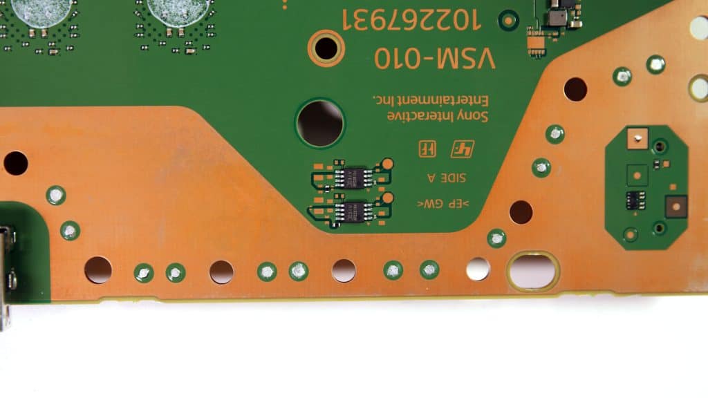
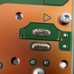
This pair of high-side power switches (AP22818A) handles the console’s USB ports.
There are VRMs everywhere on the mainboard to convert the 12V rail that the PSU supplies to various voltage levels required by the mainboard’s circuits. The primary PWM controller is by Infineon (XDPE14286A). This digital dual rail 8-phase controller is typically found in high-end desktop applications, as well as in servers and workstations.
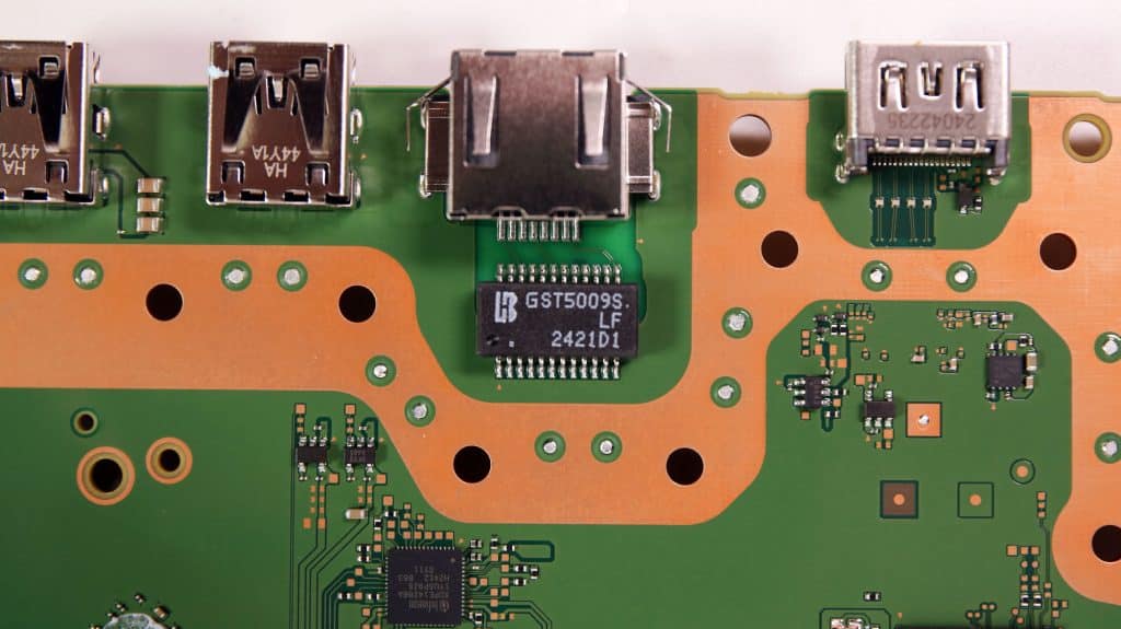
This is a 1000 Base-T Magnetics Module utilized by the consoler’s Ethernet port.
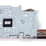
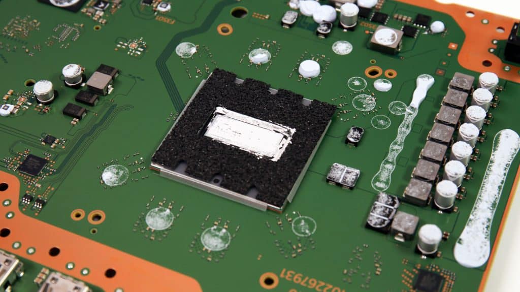
The bottom heatsink covers the APU. I removed it, of course, to give you a better look at the latter. Notice the amount of liquid metal applied on the heatsink.
This side of the mainboard hosts the APU. Notice the liquid metal on top of it. Sony decided to use liquid metal to ensure better contact of the APU with the heatsink, which means lower operating temperatures and lower noise output with the proper heatsink and fan speed profile.
The major upgrade in the PS5 Pro is in the APU. It might keep the Zen2 CPU for compatibility purposes, but it has an RDNA 3 GPU instead of the aged RDNA 2 in the previous PS5 version, which used AMD’s first-generation RT accelerators. In RDNA 3, each Compute Unit includes a ray tracing accelerator, so since the PS5 Pro’s APU has 60x CU units, it also has 60x RT accelerators. With 60x CUs, the PS5 Pro’s GPU has the same CUs as the RX 7800 XT, but it isn’t as powerful as this GPU, given the much lower number of TFLOPs that Sony states for the PS5 Pro’s GPU. It is closer to the 7700 XT.
The PS5 Pro and previous PS5 versions use a special PSU that delivers a 12V rail and high amperage. The PSU’s model number is ADP-420DR, which can provide up to 35A with 12V output or 420W. The previous PS5 versions used ADP-400DR PSUs, which deliver 20W less full power.
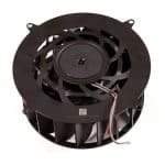
Foxconn makes the cooling fan, which has the model number PBT-GF3O. It takes 12V input and can draw up to 1.8A, so it is pretty strong.













Valorant is a competitive FPS by Riot Games. In 5v5 tactical battles, agents fight using unique abilities. Weapons and abilities can be purchased with Valorant VP Satın Al.