Intel’s 18A faces low yields and falls short of TSMC’s N2 in SRAM advancements.
Intel’s 18A node, positioned to deliver groundbreaking performance and efficiency, faces significant challenges ahead of its expected 2025 production ramp. Reports indicate that Intel is grappling with sub-10% yield rates and a critical shortfall in SRAM density compared to TSMC’s next-generation N2 process, raising questions about Intel’s ability to compete effectively.
Intel 18A’s Yield Woes: A Bottleneck to Progress
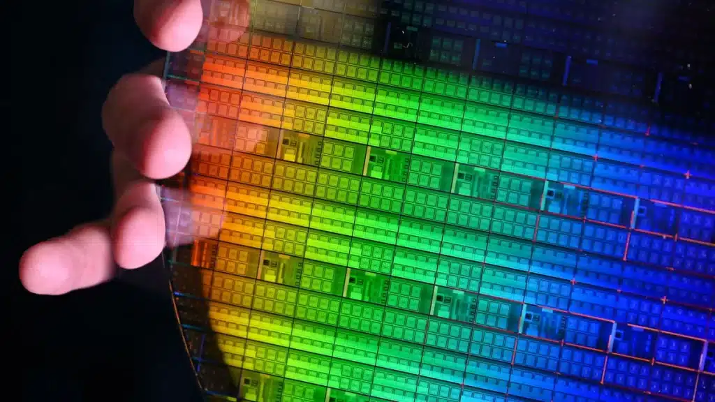
According to South Korean outlet Chosun, Intel’s 18A node yield rates currently sit below 10%, meaning nearly nine of every ten chips produced are defective. This is particularly concerning as Intel has abandoned its 20A node for Foundry customers, redirecting resources to 18A. If Intel fails to improve its yields—targeting above 60% significantly—it risks delaying its roadmap for products like Clearwater Forest server chips, Panther Lake mobile CPUs, and custom AI silicon.
While yield challenges are not unique to Intel, with Samsung’s 3nm Gate-All-Around (GAA) yields reportedly between 10% and 20%, TSMC’s dominance lies in its ability to bring processes to production efficiently.
SRAM Density: Intel Lags Behind TSMC’s N2

A major differentiator between Intel’s 18A and TSMC’s N2 processes lies in SRAM density—a key factor for chip performance and size optimization. Modern designs rely heavily on SRAM, making its density a pivotal metric for advanced process nodes.
- Intel 18A: Features a high-density SRAM bit cell size of 0.021 μm², achieving approximately 31.8 Mb/mm²—a significant improvement over Intel’s previous Intel 4 node but on par with TSMC’s older N3E and N5 technologies.
- TSMC N2: Sets a new benchmark with an SRAM bit cell size of 0.0175 μm², achieving a much denser 38 Mb/mm².
This disadvantages Intel’s 18A against TSMC’s 2nm-class process. By aggressively scaling its SRAM, TSMC enables more compact and efficient chip designs—a crucial advantage for modern processors, where SRAM demands are higher than ever.
GAA and BSPDN: Intel’s Saving Grace?
Intel’s 18A and TSMC’s N2 nodes adopt Gate-All-Around (GAA) transistor technology, allowing for tighter control over current flow and improved scaling compared to older FinFET designs. Intel, however, touts its backside power delivery network (BSPDN) as a significant advantage. BSPDN enhances power efficiency by delivering power directly to transistors, improving performance and logic density.
While Intel’s SRAM density remains a weakness, logic density—a critical aspect of process nodes—could still favor Intel’s 18A due to its BSPDN implementation. However, Intel and TSMC have not disclosed direct comparisons for logic density metrics.
Despite yield struggles, Intel remains optimistic about 18A, as it has time to refine its process before the anticipated 2025 ramp-up. For now, TSMC’s N2 holds the edge in SRAM density and its demonstrated ability to scale aggressively. If Intel hopes to remain competitive, it must resolve its yield issues while leveraging the potential benefits of GAA and BSPDN.
The competition between TSMC’s N2 and Intel’s 18A will shape the future of semiconductor innovation. Whether Intel can close the gap or whether TSMC will cement its lead remains to be seen, but for now, TSMC appears to have the upper hand.


