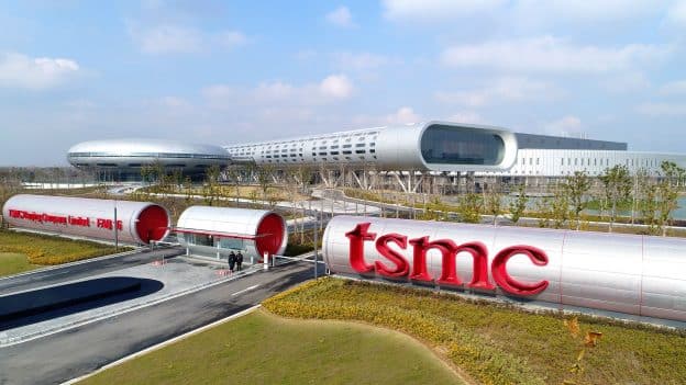
According to a Bloomberg report citing sources, TSMC’s first U.S. fab in Arizona conducted a multi-month trial production in April to produce N4 node wafers with low defect rates. The yields were reportedly comparable to those manufactured in its Southern Taiwan Science Park facility, showing promise in meeting its targets.
Addressing the matter, TSMC reportedly stated that the project is progressing as planned without further commenting on the yield. TSMC plans to build three plants in Arizona, each with cleanroom spaces twice the size of typical logic fabs in the industry. This indicates that TSMC’s expansion efforts in the U.S. are considered a success. Advanced chipmaking is a very complex process that is only done by a few makers and in a few locations. With TSMC expanding in the U.S. and proving its technology can work on U.S. soil, the company has a green light to start volume production in the first half of 2025.
The first fab is expected to begin mass production in the first half of 2025. TSMC’s second fab in Arizona will use 2nm process technology to meet AI-related solid demand, with production expected to begin in 2028. The third fab in Phoenix will employ a 2nm or an even more advanced process. TSMC stated that once the fabs are fully operational, they will deliver the same manufacturing quality and reliability level in Arizona as in its Taiwan facilities.
In April, the U.S. government officially announced that it would provide a USD 6.6 billion subsidy to TSMC. It confirmed that TSMC will build its third fab in Arizona, USA, with total investment rising to USD 65 billion. If upcoming fabs follow the lead of the first facility, US-based production needs can be satisfied.
Sources: TechPowerUp.com, Trendforce.com


