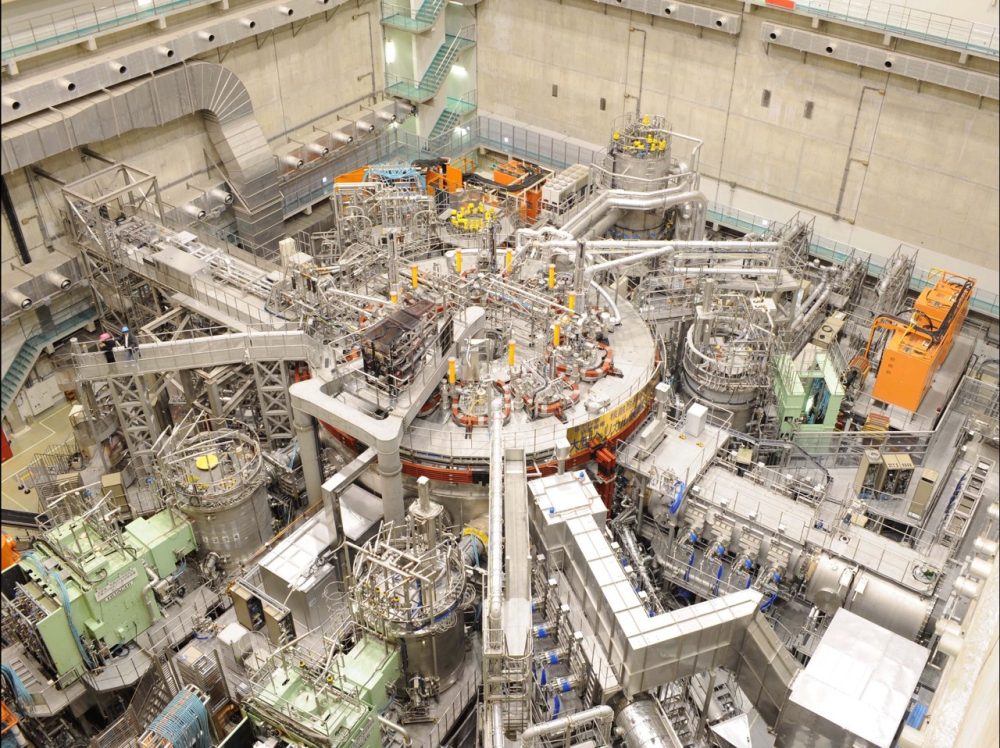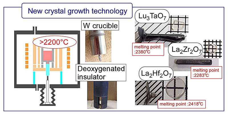
Semiconductors, optical devices, and scintillators all rely on single crystals, but until now, these crystals have had a fundamental weakness: they can’t take extreme heat. Materials like iridium and platinum, commonly used in crystal growth, have melting points below 2,200°C, creating a hard ceiling for next-generation devices.
Researchers at Tohoku University’s Institute for Materials Research have smashed through that barrier. Associate Professor Yuui Yokota and Professor Akira Yoshikawa have developed a groundbreaking tungsten-based crystal growth technology that works at temperatures above 2,200°C.
The challenge was immense. Tungsten (W) has a high melting point, but it usually reacts with oxide materials or contaminates the crystals. The team overcame this by designing a method that suppresses unwanted reactions and prevents contamination, unlocking the ability to grow high-density single crystals far beyond the quality of existing scintillators.
The implications are wide-ranging:
- Medical Imaging: PET scanners using these crystals could detect early-stage cancers faster and more accurately.
- Electronics & Semiconductors: Devices that withstand extreme heat could become more efficient and durable.
- Optics & Sensors: New materials with higher band gaps could fuel advanced lasers, sensors, and detectors.
- Piezoelectrics: High-performance crystals could expand applications in aerospace, energy, and robotics.
Published in Scientific Reports, the study not only proves the concept but also outlines a roadmap toward mass production, with support from the Japan Science and Technology Agency (JST).
“This breakthrough means we can now create a plethora of new materials for a wide range of applications,” said Yoshikawa.
By crossing the 2,200°C threshold, the Tohoku team has opened the door to an entirely new materials frontier, one that could redefine the future of semiconductors and beyond.