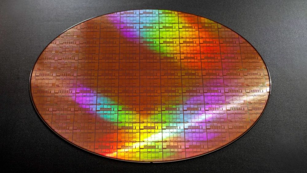
Japanese semiconductor manufacturer Rapidus has officially entered the 2nm era. The company announced that it has begun test wafer production featuring gate-all-around (GAA) transistors at its IIM-1 fab in Chitose, marking a significant milestone in Japan’s efforts to regain its position as a global leader in chipmaking.
Notably, Rapidus is committing to single-wafer processing for every front-end step, a bold departure from the mixed-method approaches employed by established giants like TSMC, Intel, and Samsung.
2nm GAA Prototyping Now Underway
Test wafers are now in circulation at the IIM-1 fab, and initial measurements show that electrical characteristics are aligning with expectations. The wafers include circuits built with GAA transistor structures, a next-generation architecture that promises higher performance and energy efficiency compared to FinFET.
Among the key parameters being evaluated are:
- Threshold voltage
- Drive and leakage current
- Subthreshold slope
- Switching speed and power consumption
- Capacitance
While Rapidus hasn’t disclosed specific numbers, the early success indicates that critical tools, including DUV and EUV lithography systems, are operating as planned.
Construction of IIM-1 commenced in September 2023, with the completion of the clean room scheduled for 2024. As of June 2025, over 200 tools have been installed, including EUV systems delivered in late 2024 and the first exposed wafers processed in April 2025.
Commitment to Single-Wafer Processing
In a significant strategic move, Rapidus has confirmed that all front-end processes at IIM-1 will be conducted using single-wafer processing from oxidation and ion implantation to etching, deposition, cleaning, and annealing.
This approach, while more complex and expensive than batch processing, offers several critical advantages:
- Real-time, per-wafer optimization
- Early anomaly detection
- High-resolution data collection
- Greater adaptability for small-volume and specialty production
By treating each wafer as its dataset, engineers can dynamically fine-tune processes, improving yields and reducing defects more efficiently. This high-volume, high-granularity data stream is also well-suited to AI-driven process control, enabling faster continuous process improvements (CPI) and tighter statistical process control (SPC).
Lower throughput per tool, longer production cycles, and higher capital costs. But for Rapidus, which is targeting high-value, small-batch production for specialized customers, the precision and agility offered by single-wafer processing could be a long-term differentiator, especially at the 2nm node and below.
PDK and Design Infrastructure Coming in 2026
Looking ahead, Rapidus is preparing to release its first Process Design Kit (PDK) in Q1 2026, a key milestone that will enable customer design work. The company is also building out design prototyping infrastructure at IIM-1 to support early partners and tap into the global ecosystem of chip designers.
A Strategic Leap for Japan’s Semiconductor Renaissance
With 2nm prototyping now underway and a forward-thinking manufacturing strategy in place, Rapidus is positioning itself as more than just a contract fab; it’s aiming to become a precision partner for next-generation chip design.
The challenge remains steep: catching up to TSMC and Samsung won’t happen overnight. But if successful, Rapidus could offer something those giants don’t: tailored, AI-optimized, high-precision production with full control at every step.