China is attacking the semiconductor race on two fronts at once: by shrinking today’s chipmaking tools and leapfrogging tomorrow’s chip designs.
Desktop-Sized EUV Light Source For 14 nm Chips
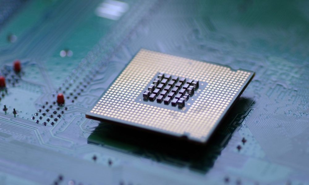
At the UltrafastX conference in late October, Hefei Lumiverse Technology, based in Anhui province, unveiled a desktop-sized extreme ultraviolet (EUV) light source. That’s remarkable because EUV is normally associated with huge, building-sized, ultra-expensive systems used by only a few of the world’s top fabs.
Instead of chasing the bleeding edge, Lumiverse is targeting the high-volume, high-value 14 nm node. While not cutting-edge anymore, 14 nm chips are still a workhorse for sectors like:
- Industrial automation
- Electric vehicles
- Smart wearables and IoT
By shrinking EUV sources to fit in a lab or factory floor, China could lower the cost and complexity of producing these mainstream chips and reduce its reliance on imported tools. It also fits perfectly with Beijing’s broader goal: build a domestic, vertically integrated semiconductor supply chain, especially as SMIC and other local fabs push 14 nm and even 7 nm production using as much Chinese equipment as possible.
Lithography, however, remains the hardest part. Most production lines still depend on ASML and Nikon machines, often older models, because no Chinese vendor has yet offered a competitive full-lithography system. Lumiverse’s compact EUV source doesn’t solve that alone, but it’s a sign that China is chipping away at the gap one critical component at a time.
A Photonic Chip That Computes With Light, Not Electrons
In parallel, Chinese researchers are also aiming beyond silicon entirely. A team from Tsinghua University and the Institute of Microelectronics has developed a prototype photonic chip that uses light (photons) instead of electricity (electrons) to process data.
According to early reports, this chip:
- Uses nanophotonic waveguides to route light through the processor
- Reaches speeds above 1 petahertz (10¹⁵ operations per second) in lab tests
- Consumes less than 1% of the energy of today’s leading CPUs and GPUs
If these numbers hold up outside the lab, it would be a massive performance and efficiency leap, with obvious implications for:
- AI training and inference
- Cloud data centers
- Autonomous systems
- High-speed secure communications
The project is still in the prototype stage, with mass production targeted “within the next few years” as part of the “Made in China 2030” tech roadmap. But the message is clear: China doesn’t just want to catch up in conventional chips, it wants to define the next platform for high-performance computing.
Strategy: Fill Today’s Gaps, Define Tomorrow’s Rules
From SMIC ramping 14 nm and 7 nm under sanctions, to desktop EUV sources, to photonic architectures that sidestep many silicon limits, China is executing a dual-track strategy:
- Short term: Reduce dependency on foreign tools and nodes like EUV lithography while securing domestic capacity for 14 nm and above.
- Long term: Invest heavily in post-silicon technologies that could reset the playing field in computing power and energy efficiency.
If successful, the next era of high-performance chips might not be defined only in nanometres and transistors, but in photons, waveguides, and who controls the tools that make them.