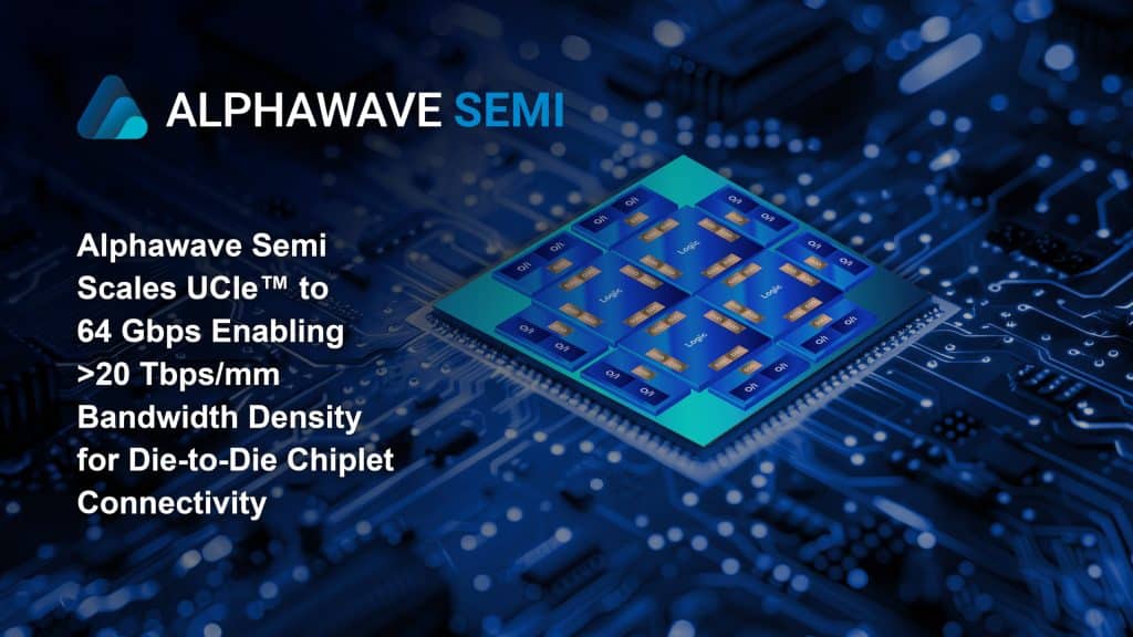
Alphawave Semi has announced its Gen3 UCIe Die-to-Die (D2D) IP subsystem, which elevates chipset interconnect speeds to an industry-first 64 Gbps. Building on the company’s successful Gen2 UCIe IP at 36 Gbps, this next-generation technology offers breakthrough performance and versatility for high-performance computing (HPC), data centers, and AI applications.
High Bandwidth Density and Scalability

Operating at 64 Gbps, the Gen3 UCIe IP subsystem achieves a remarkable bandwidth density of over 20 Tbps/mm, setting a new benchmark for die-to-die communication. The design maintains ultra-low power consumption and latency, ensuring seamless integration in disaggregated systems. Moreover, the configurable subsystem supports multiple industry protocols, including AXI-4, AXI-S, CXS, CHI, and CHI-C2C, making it suitable for various applications requiring high-performance connectivity.
The Gen3 IP complies with the latest UCIe specifications, ensuring scalability and interoperability. It also introduces advanced testability features such as live per-lane health monitoring, enhancing system reliability and performance.
Packaging Versatility
The Gen3 subsystem supports high-yield, low-cost organic substrates, and advanced packaging technologies. This flexibility is a critical advantage, as it allows customers to adopt cutting-edge interconnect solutions while optimizing for cost and manufacturing yield. Additionally, UCIe D2D interconnects facilitate low-latency, coherent links between compute and I/O chiplets and enable reliable optical I/O connections.
Proven Innovation on TSMC’s 3nm Technology
Alphawave Semi’s announcement follows the successful tape-out of its Gen2 UCIe IP at 36 Gbps using TSMC’s 3nm process technology. This milestone underscores the company’s expertise in developing silicon-proven solutions, such as its UCIe IP with CoWoS packaging.
“Our successful tapeout of the Gen2 UCIe IP at 36 Gbps on 3-nm technology builds on our pioneering silicon-proven 3-nm UCIe IP with CoWoS packaging,” said Mohit Gupta, Senior Vice President and General Manager of Custom Silicon & IP at Alphawave Semi. “This achievement sets the stage for our Gen3 UCIe IP at 64 Gbps, which is on target to deliver high performance and 20-Tbps/mm throughput functionality to our customers who need maximized shoreline density for critical AI bandwidth needs in 2025.”
Revolutionizing Chiplet Ecosystems
Alphawave Semi’s Gen3 UCIe IP is designed to support the evolving requirements of disaggregated systems, enabling next-generation chipset ecosystems. The company’s focus on scalability, interoperability, and reliability positions its technology as a game-changer for industries that demand unprecedented performance and bandwidth density.
With the Gen3 UCIe IP subsystem, Alphawave Semi reinforces its leadership in advanced semiconductor IP and paves the way for the future of chipset connectivity. Customers seeking to meet the critical bandwidth requirements of AI and HPC applications can expect the technology to be a cornerstone of innovation in 2025 and beyond.
Source:awavesemi.com


