
Part Analysis
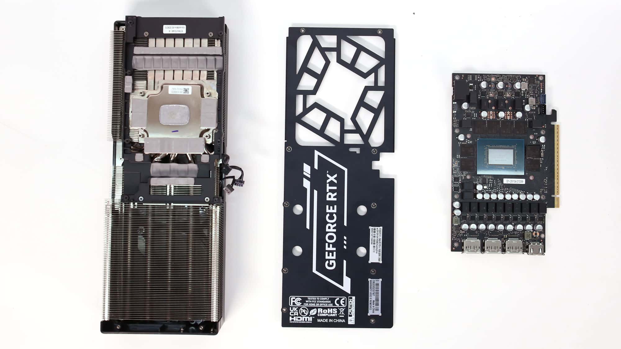
The main parts of the graphics card are the backplate, the cooler, the PCB, and the fan assembly. The cooling solution uses seven heatpipes, which pass through the block that comes in contact with the GPU.
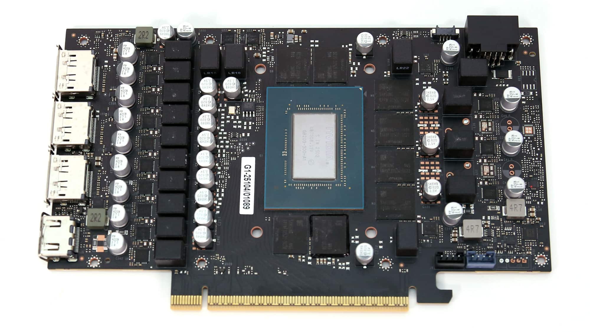
Here are photos of the PCB’s front side. It is the same size as the Galax RTX 5080 model.
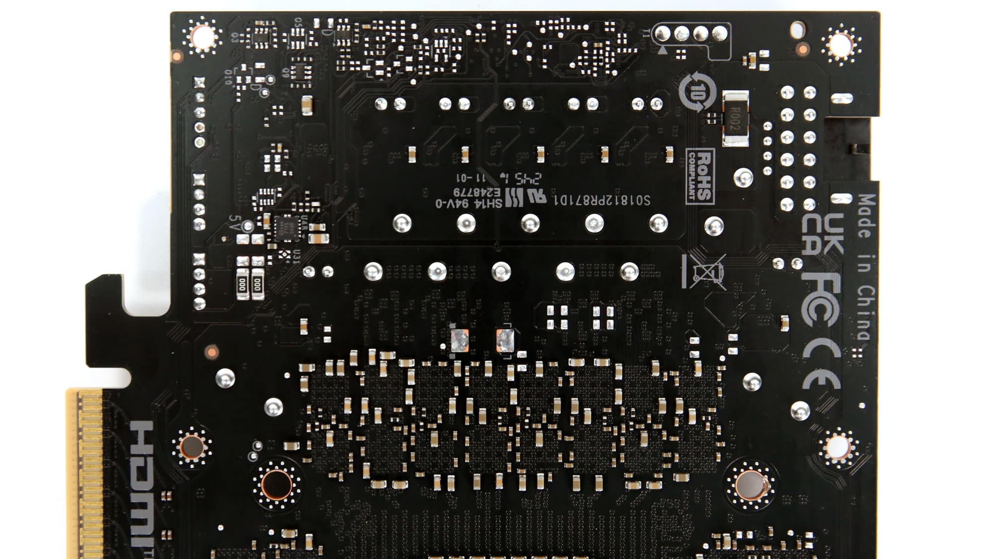
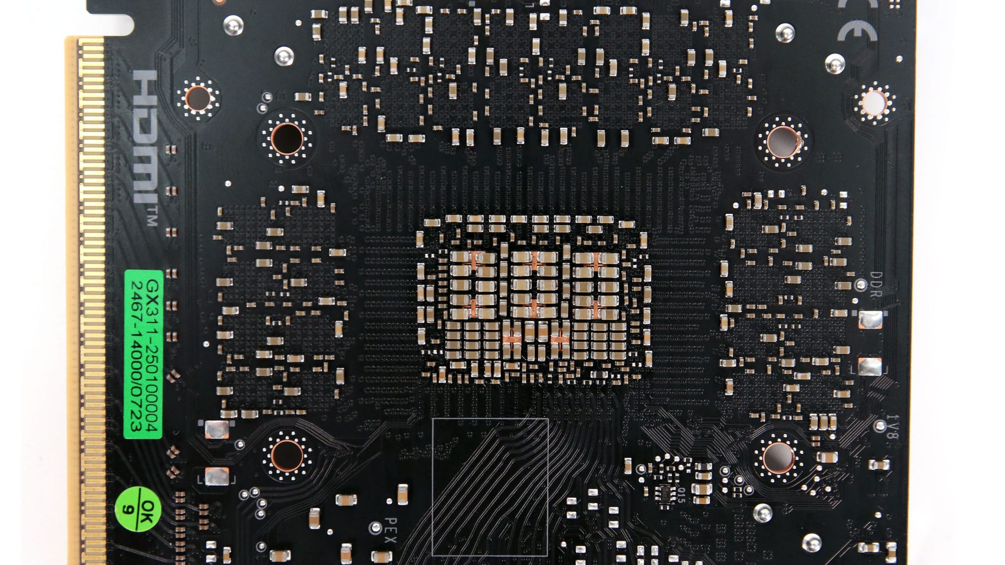
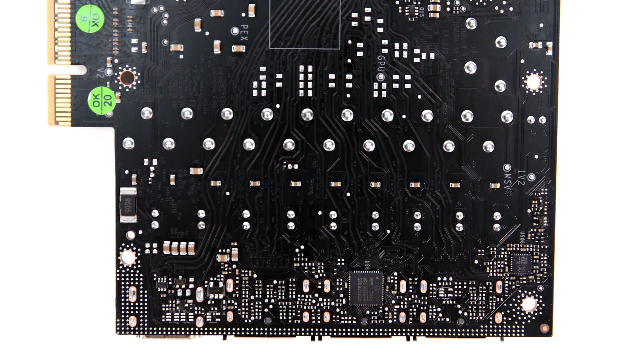
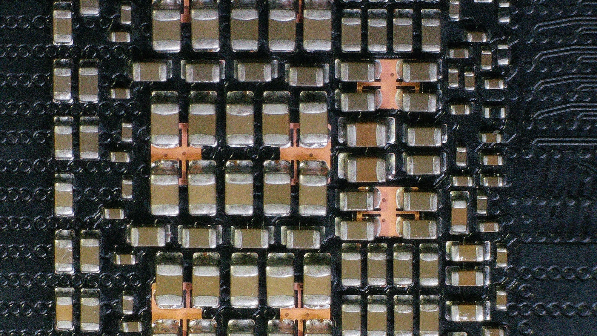
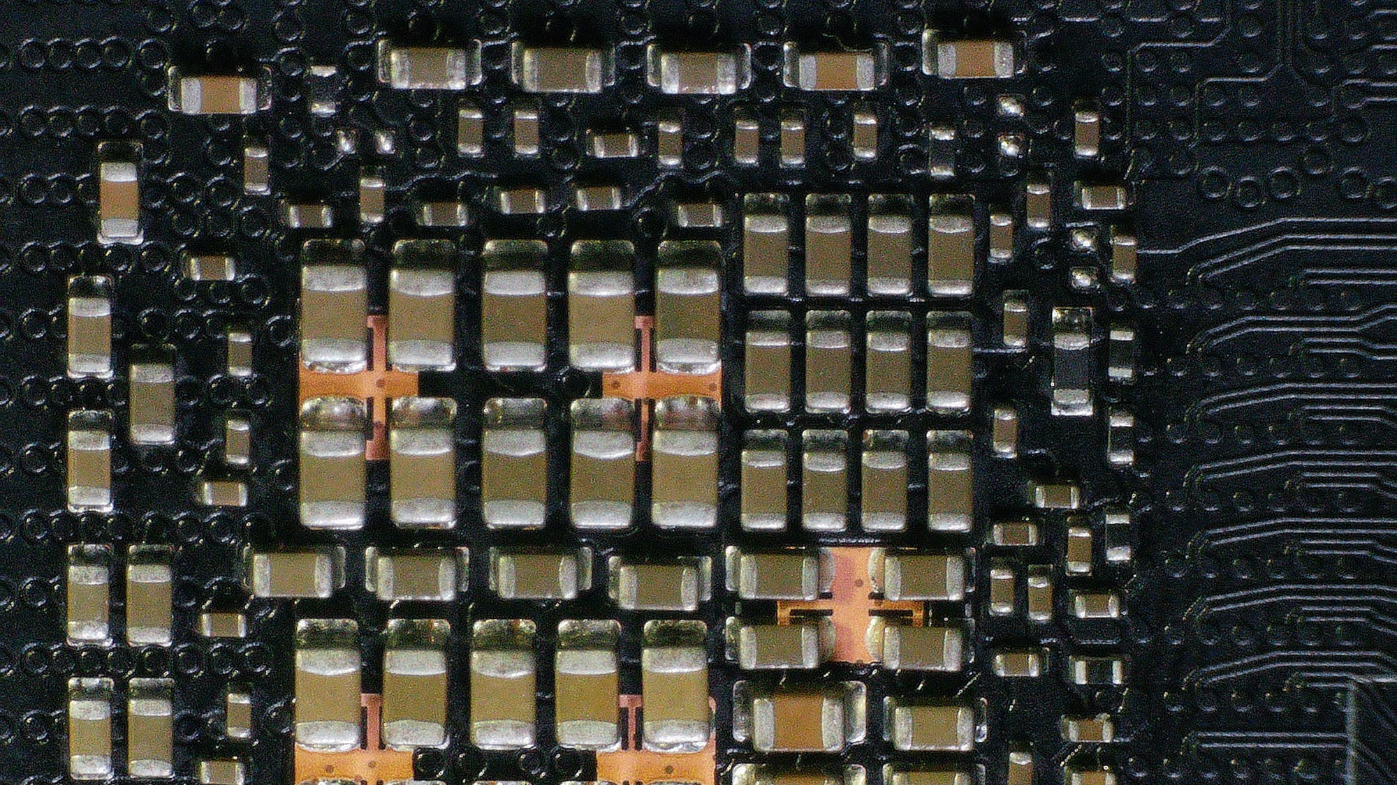
The PCB’s solder side.
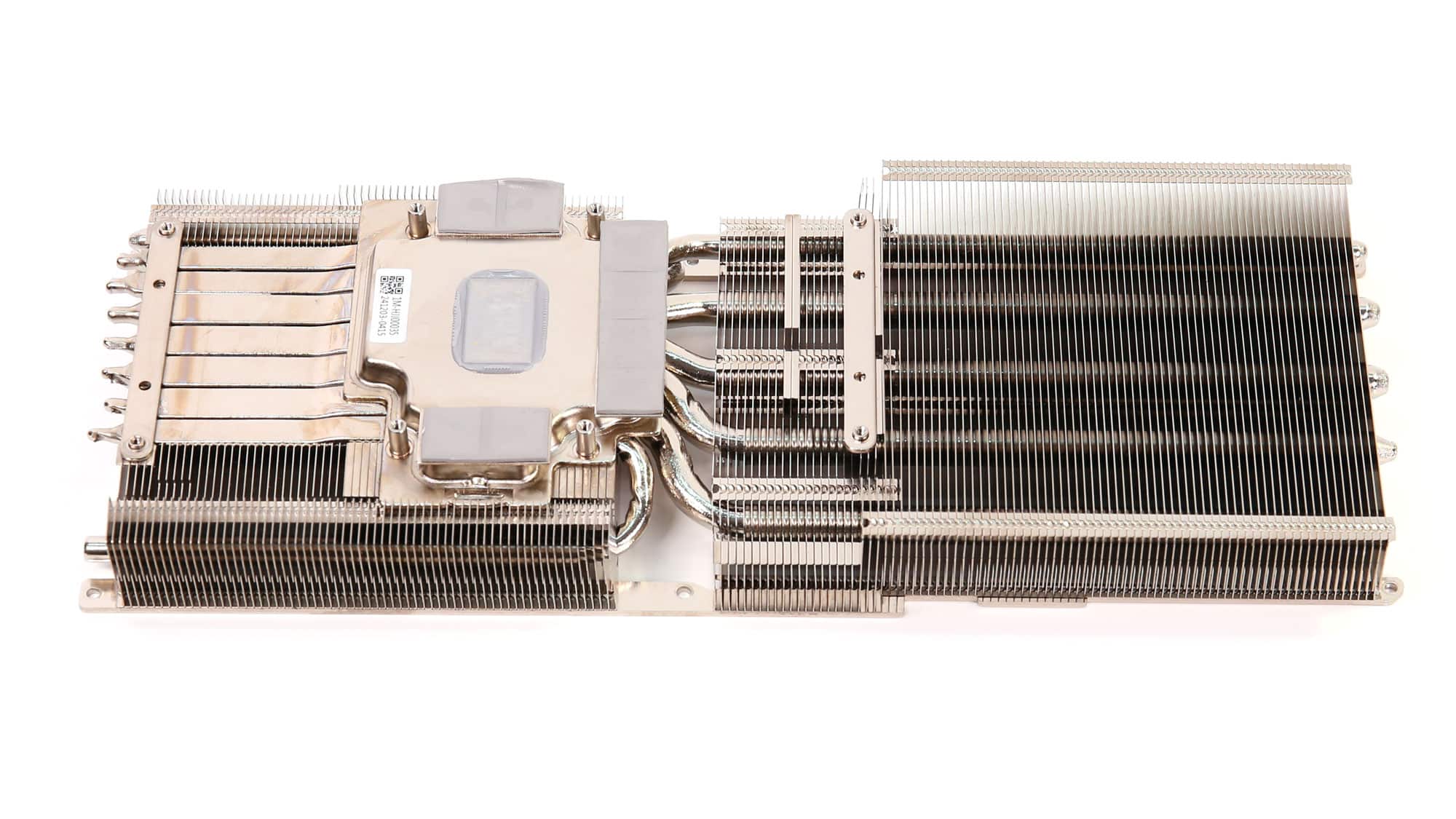
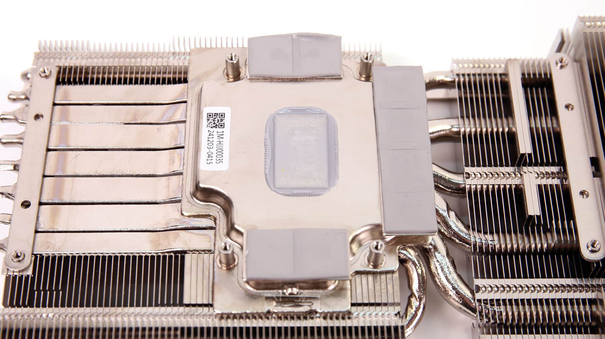
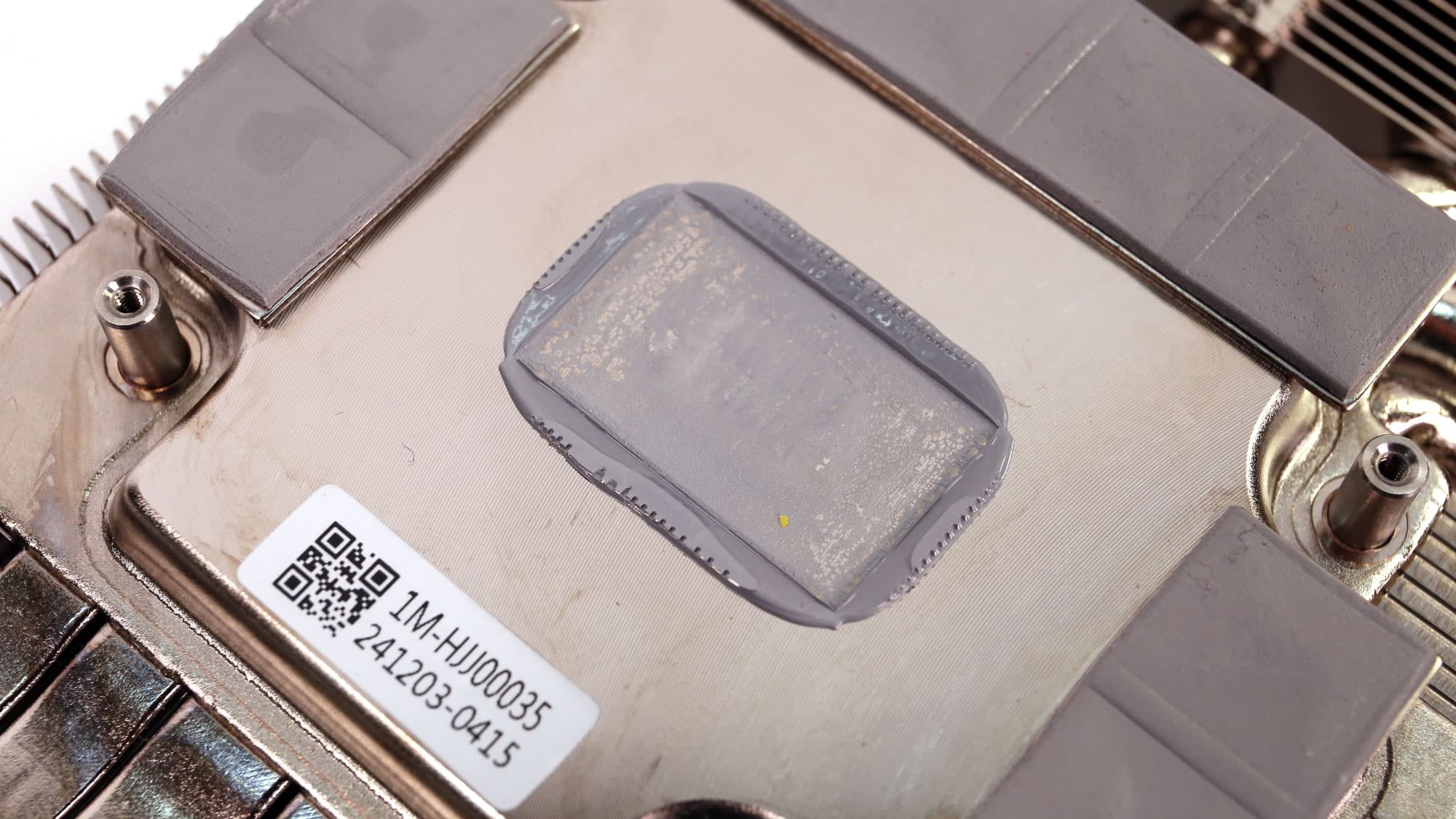
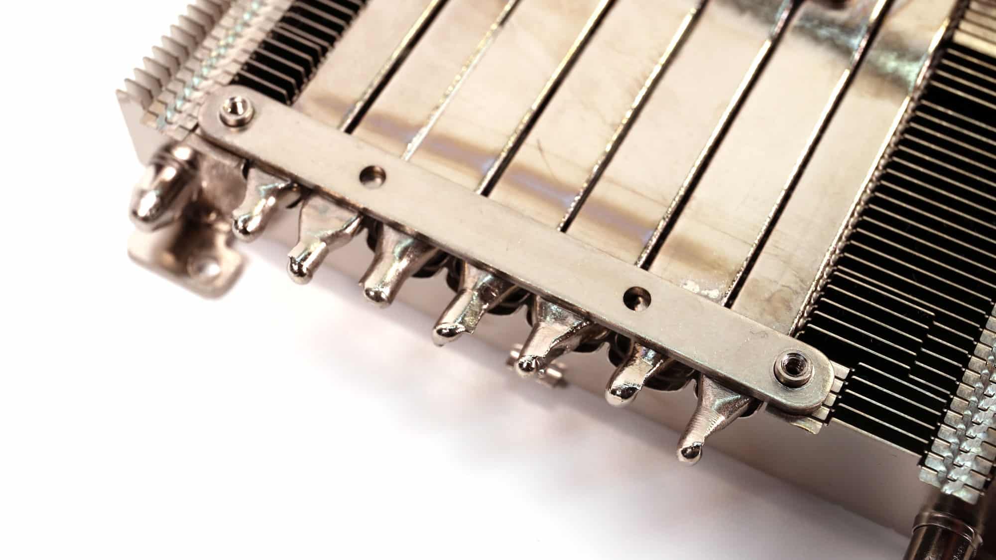
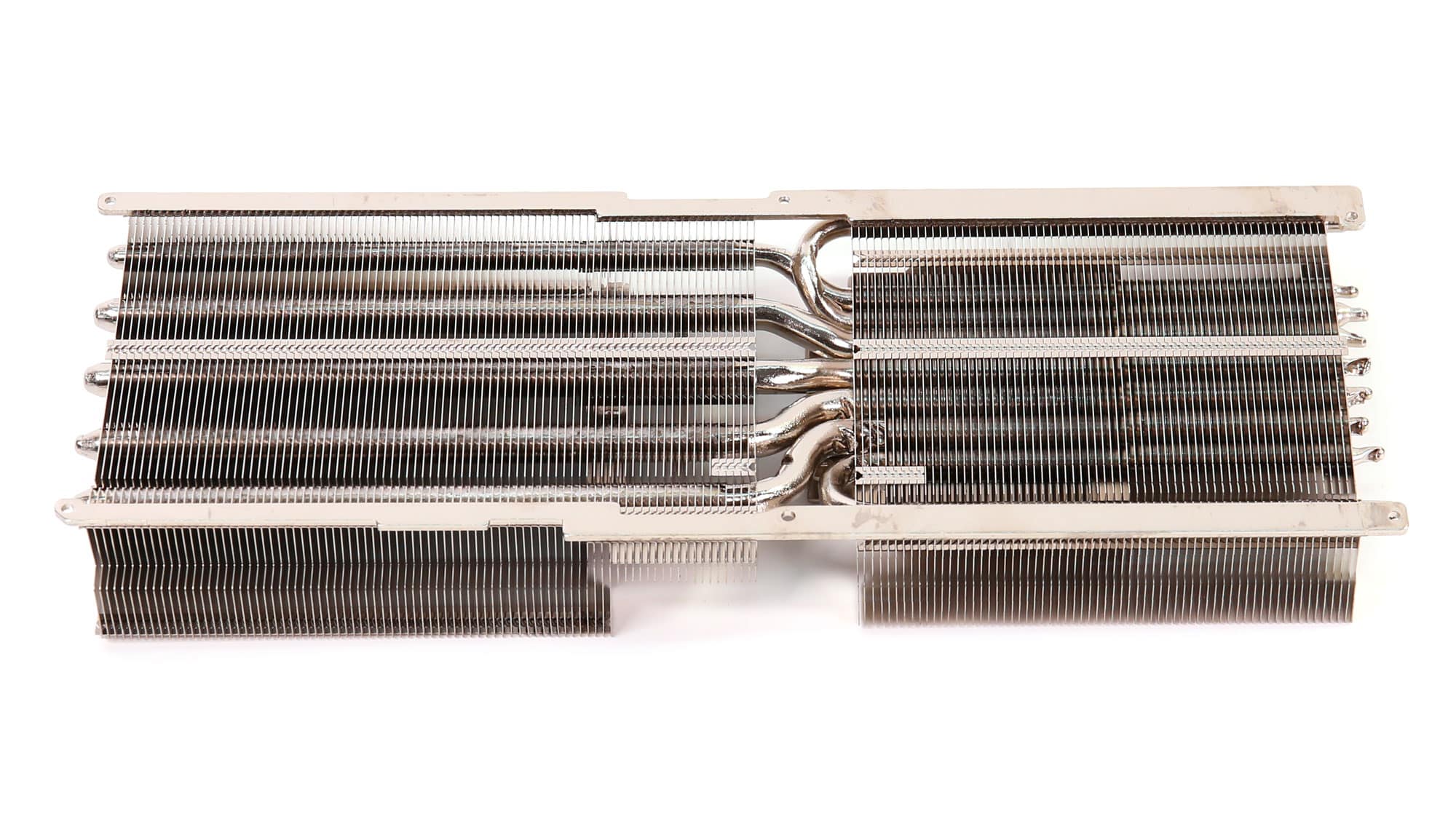
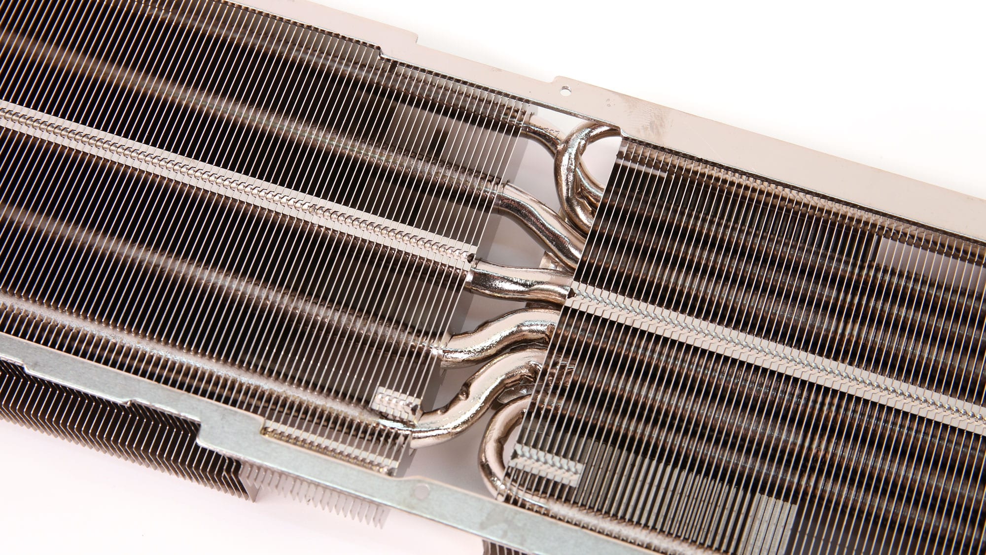
The cooling solution uses seven heatpipes, which pass through the block that comes in contact with the GPU.
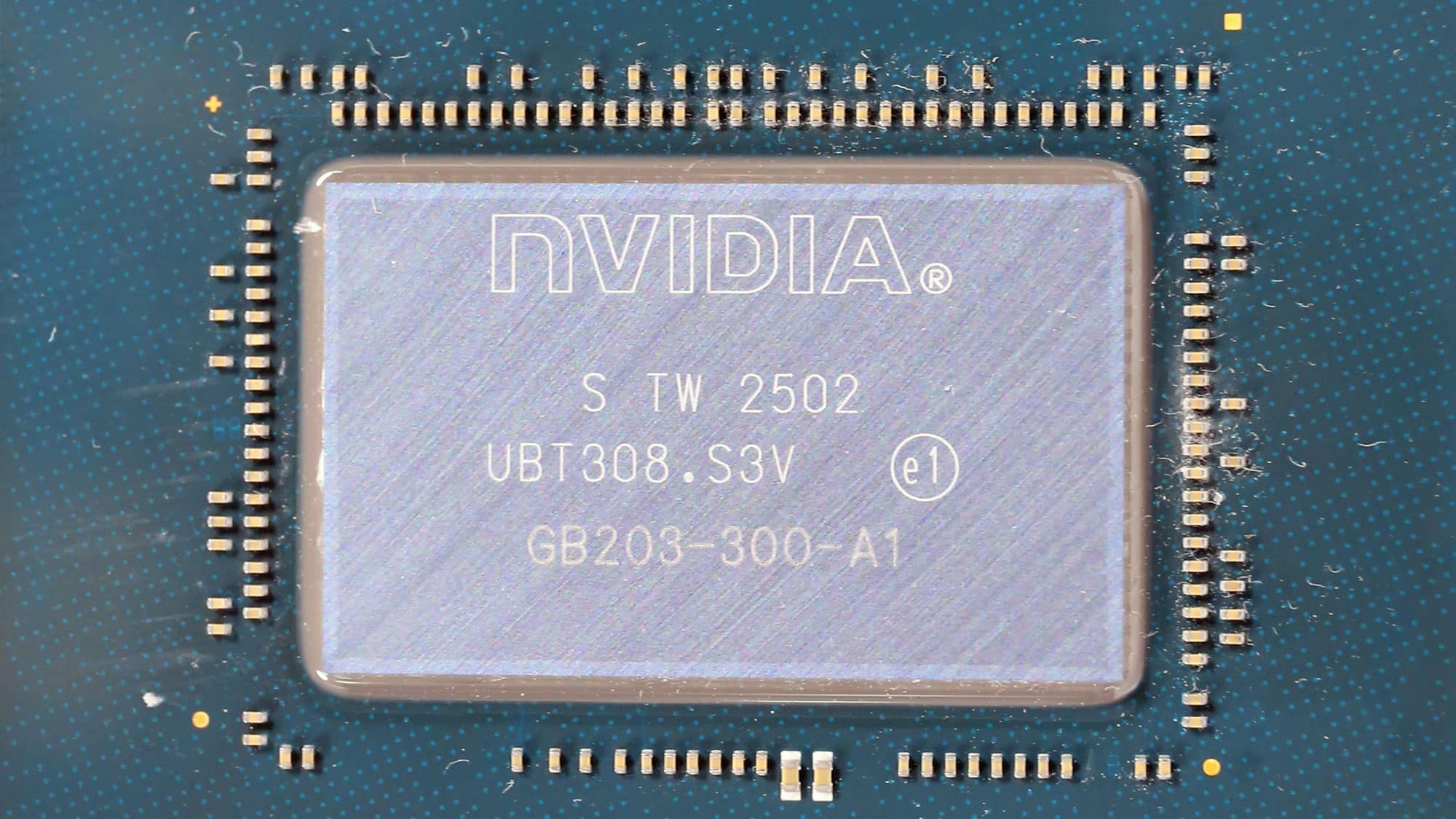
The GPU203 follows the Blackwell architecture. Like its predecessor, it is manufactured by TSMC and uses a 5 nm production process. Its die size is 378 mm2, and it has 45.6 billion transistors. It has almost the same die size as the AD103, used in the RTX 4080, and the same number of transistors (45.6 billion).
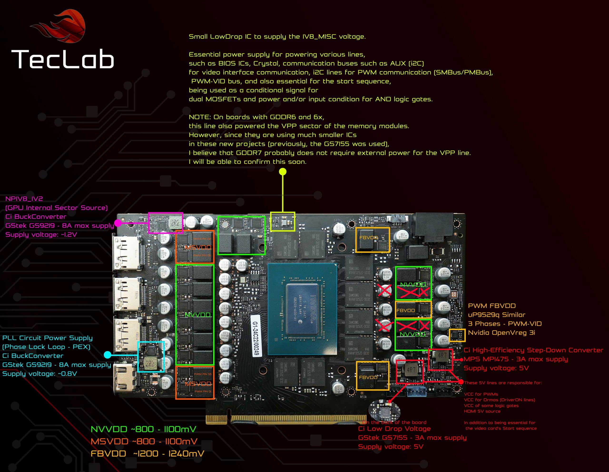
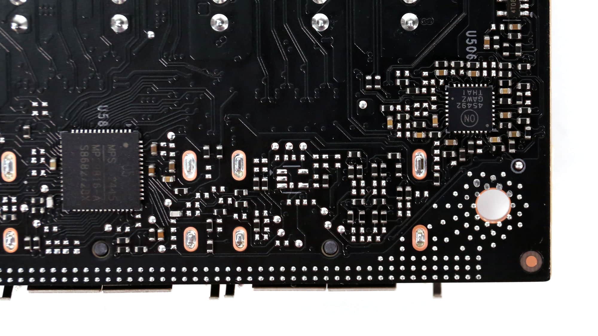
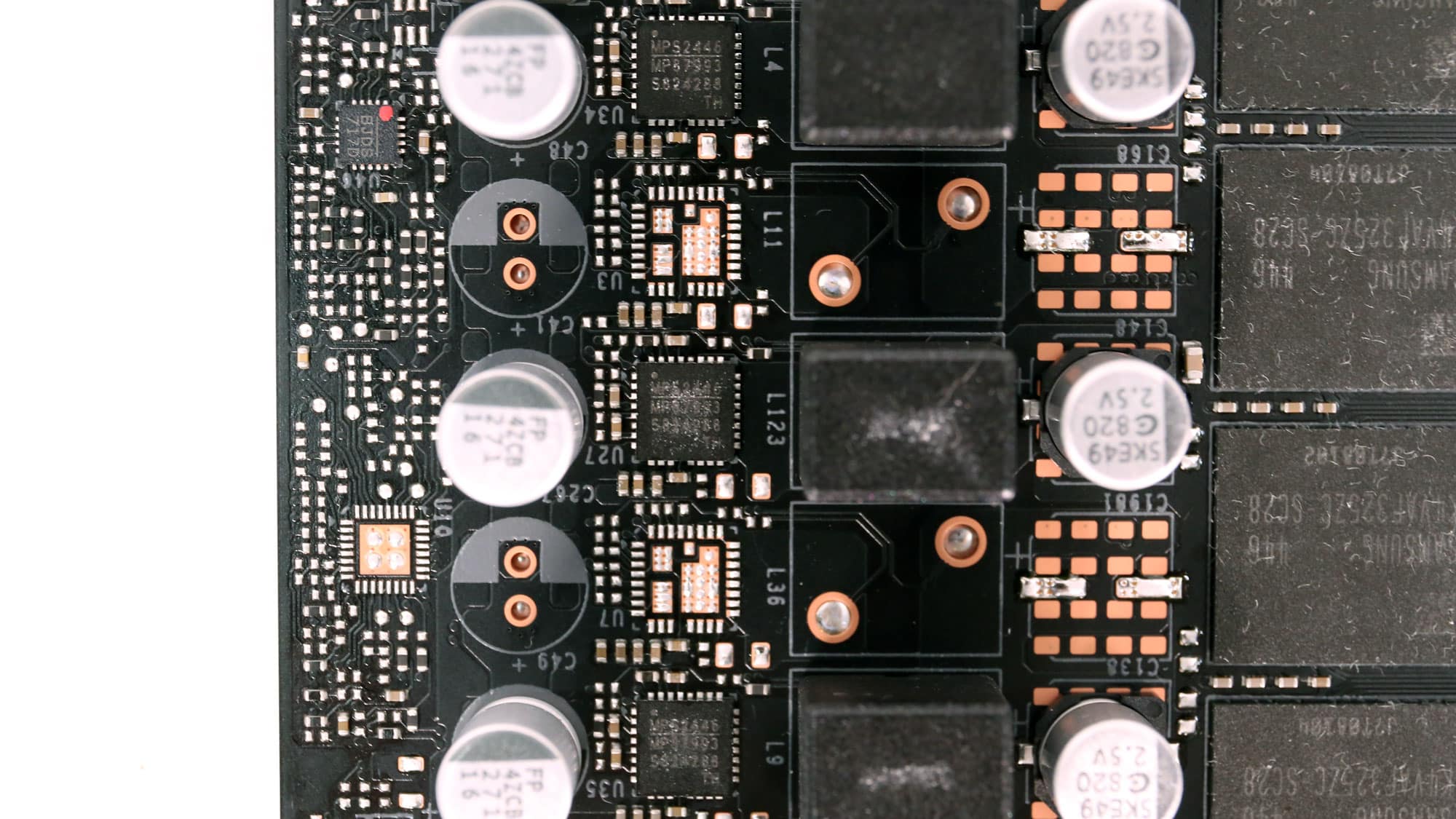
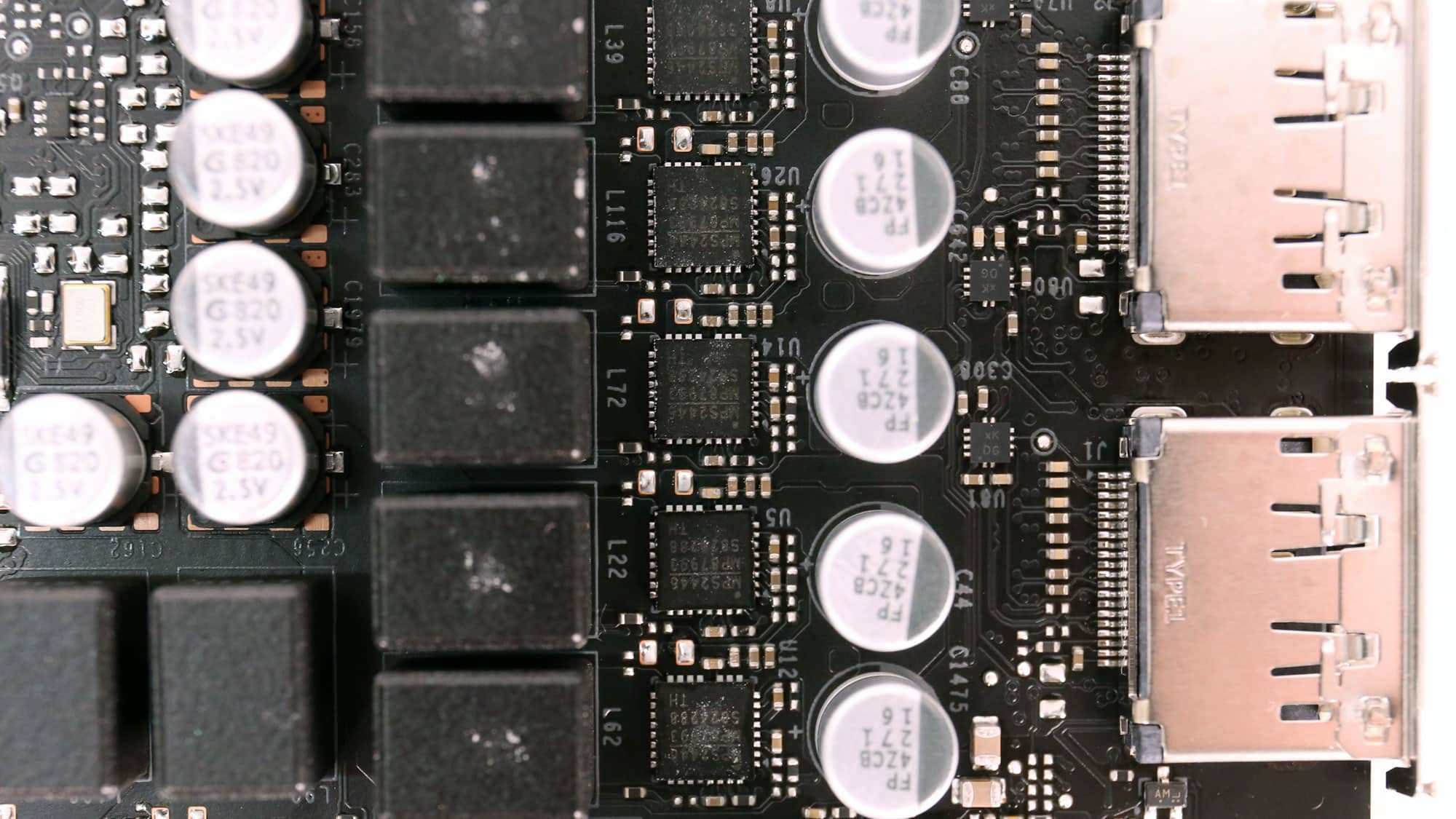
This image explains EVERYTHING you need to know about this graphics card and its power circuits. My friends at TecLab (thanks, Ronaldo and Burti), experts in GPUs and more, provided it! All credit for this part analysis goes to my friends at TecLab, who also trained me on how to do that properly!
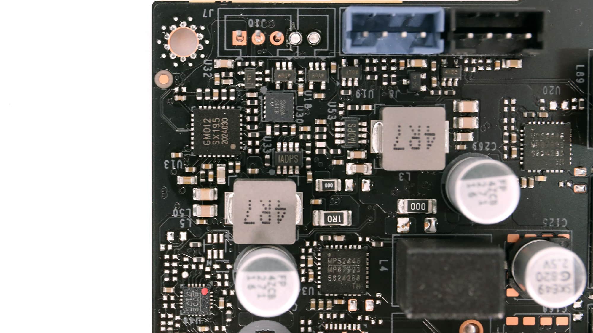
The main difference between the Galax RTX 5080 board and the RTX 5080 model is that the latter has two fewer NVVDD phases (8x in total instead of 10x on the RTX 5080 model).
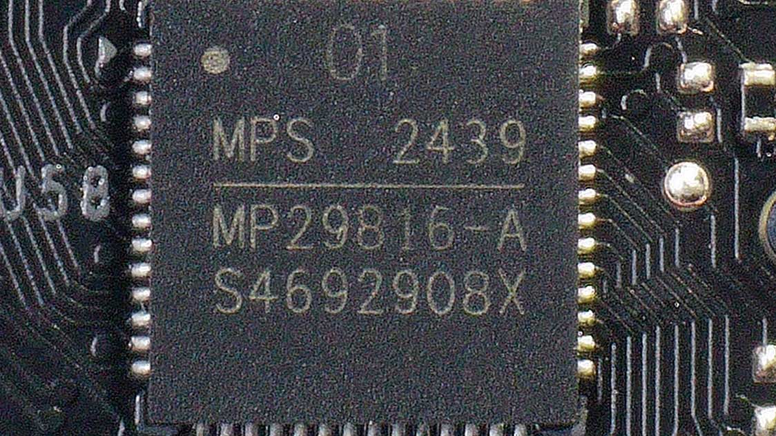
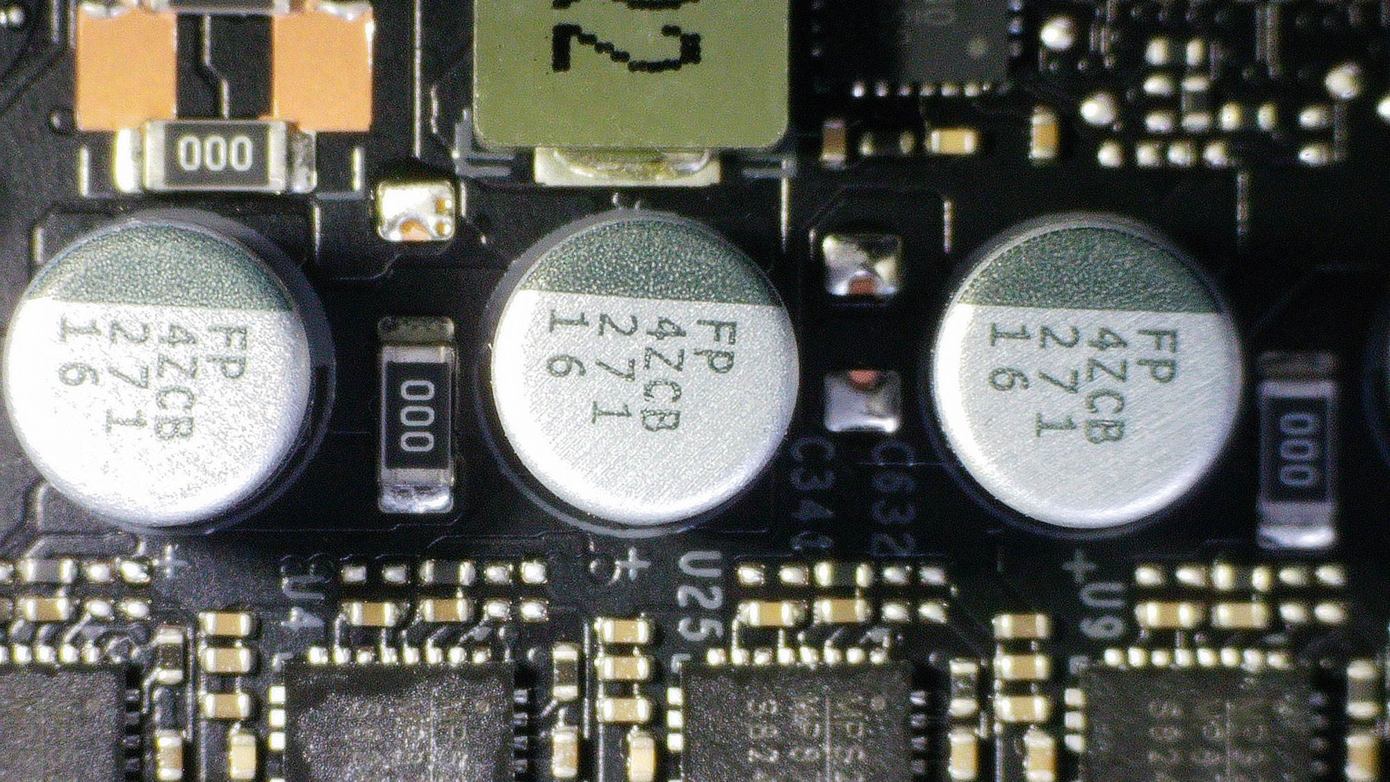
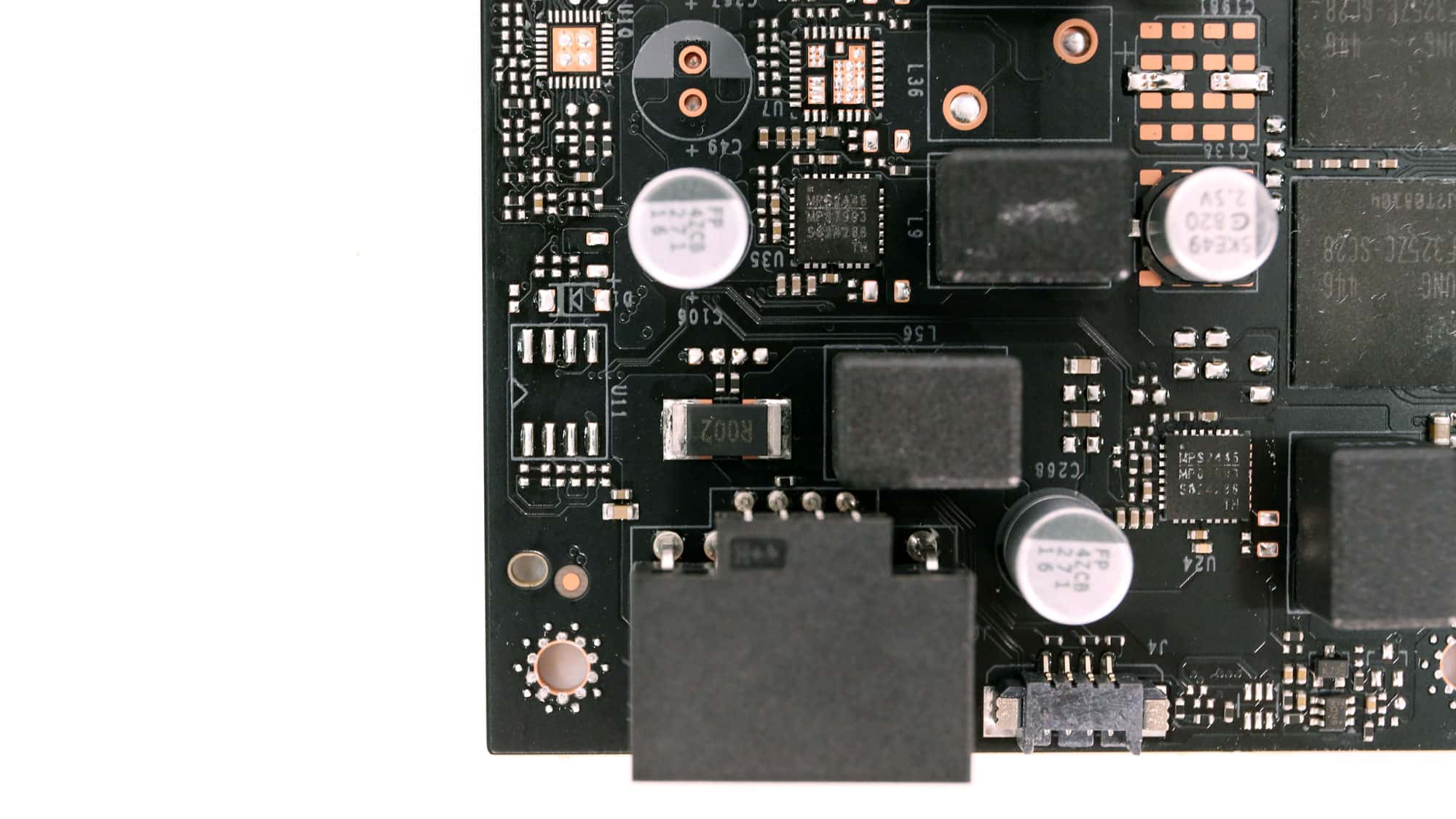
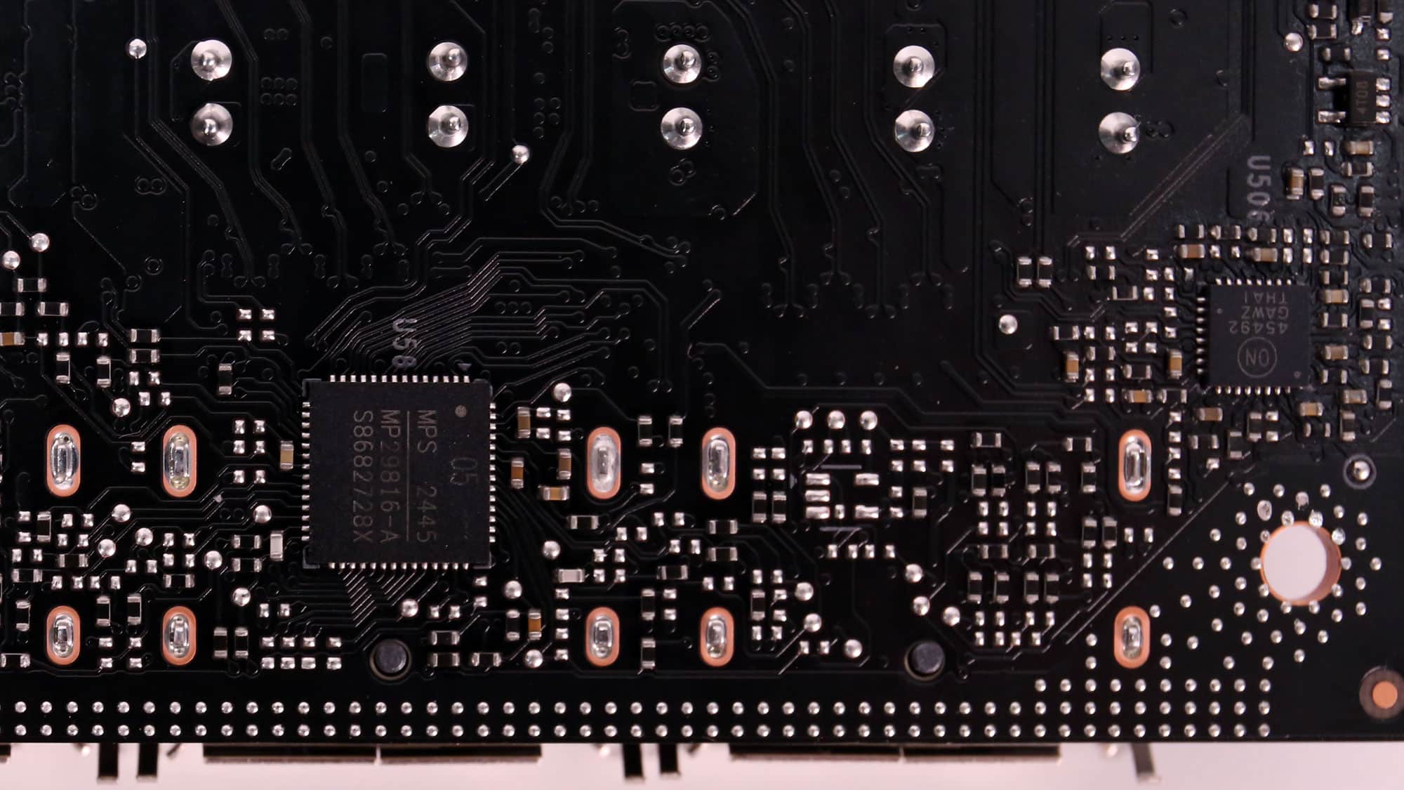
An 8-phase VRM powers the GPU, highlighted in the green rectangles above. A Monolithic Power Systems MP29816 controller controls these. There are four phases for MSVDD and three phases for FBVDD. For those who don’t know what these two mean, FBVDD ensures the stability and accuracy of data transfers between the GPU and memory, especially at high clock speeds. In contrast, the MSVDD voltage manages the memory chips’ operation.
 |
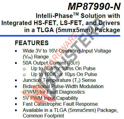 |
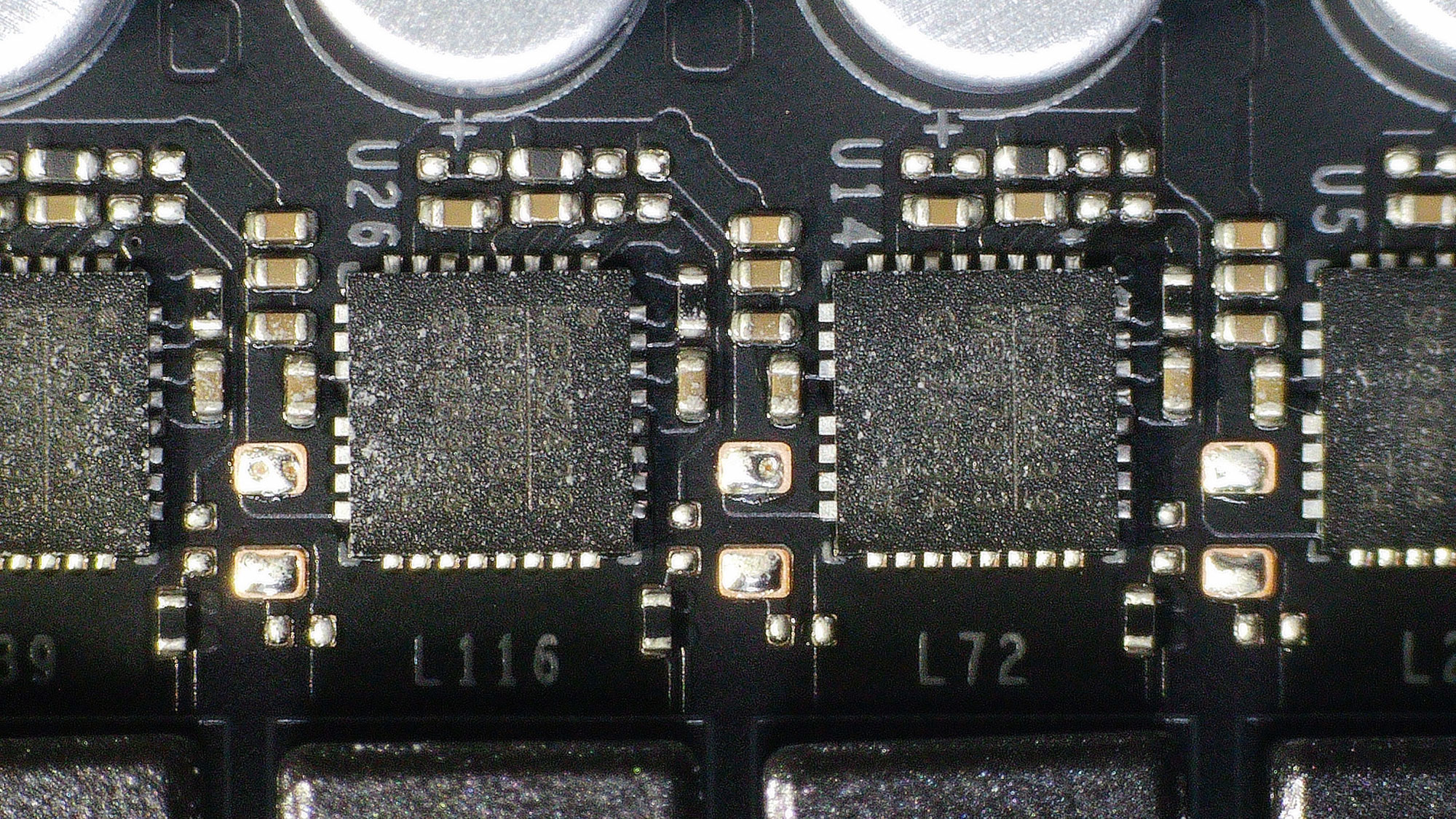
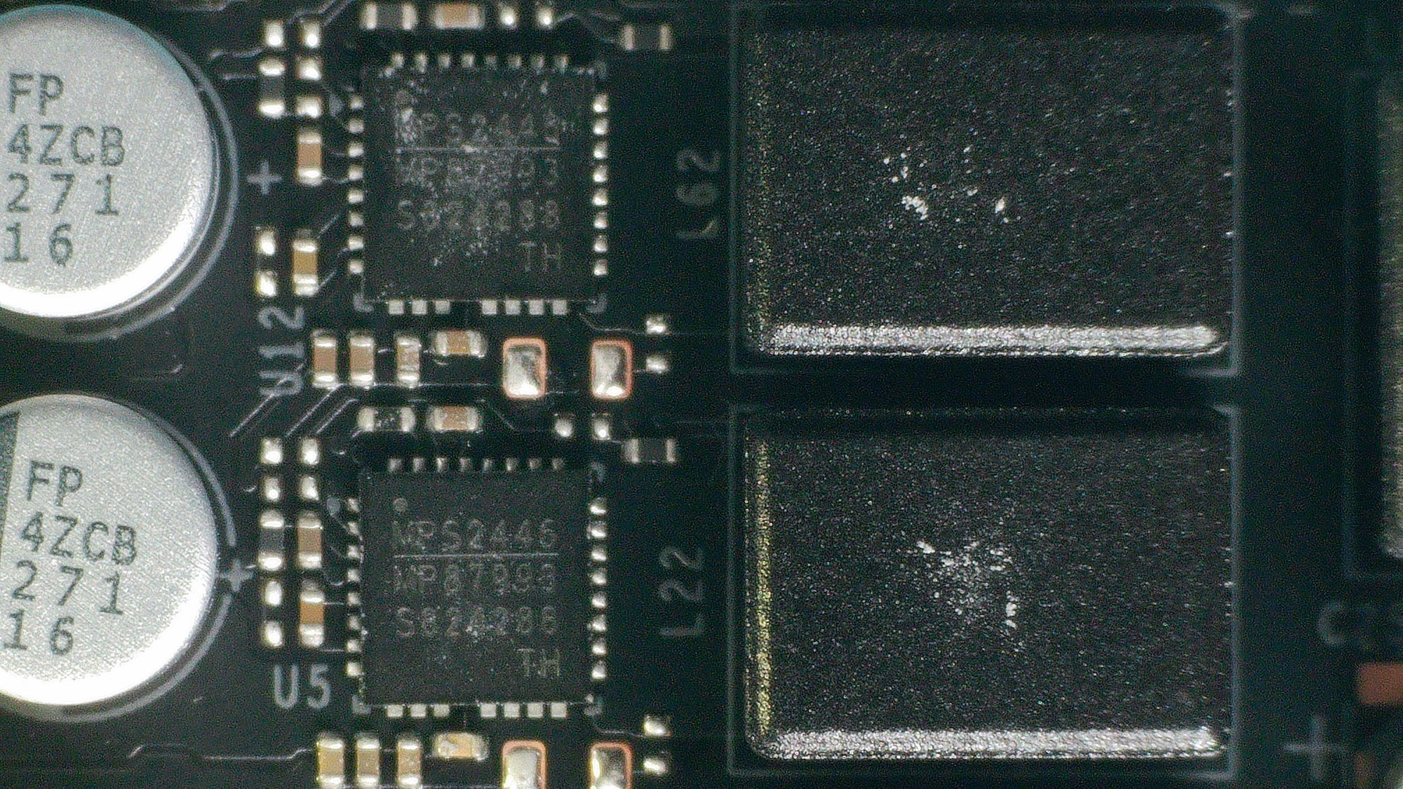
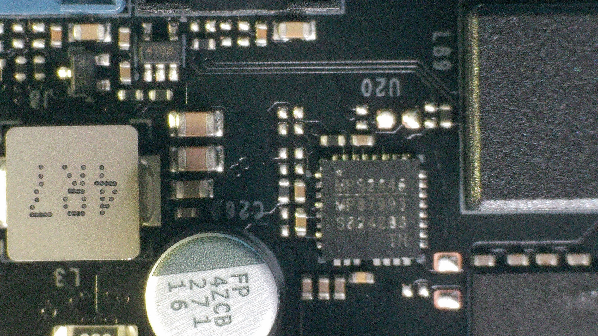
The GPU power phases use Monolithic MPS MP87993 DrMOS rated at 50A, and the VRAM phases use the same type of DrMOS.
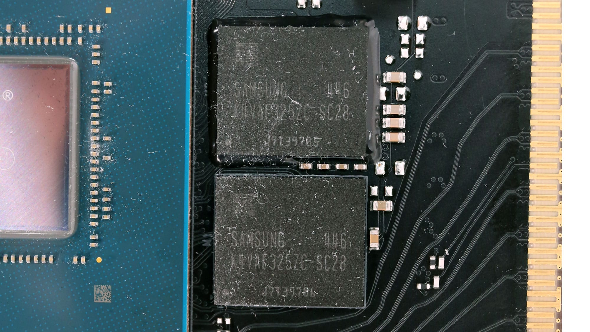
Samsung makes the GDDR7 memory chips. Their model number, K4VAF325ZC-SC28, indicates that they are rated for 28 Gbps. The RTX 5090 uses the same memory chips, while the 5080 has higher-speed rated ones (32 Gbps).
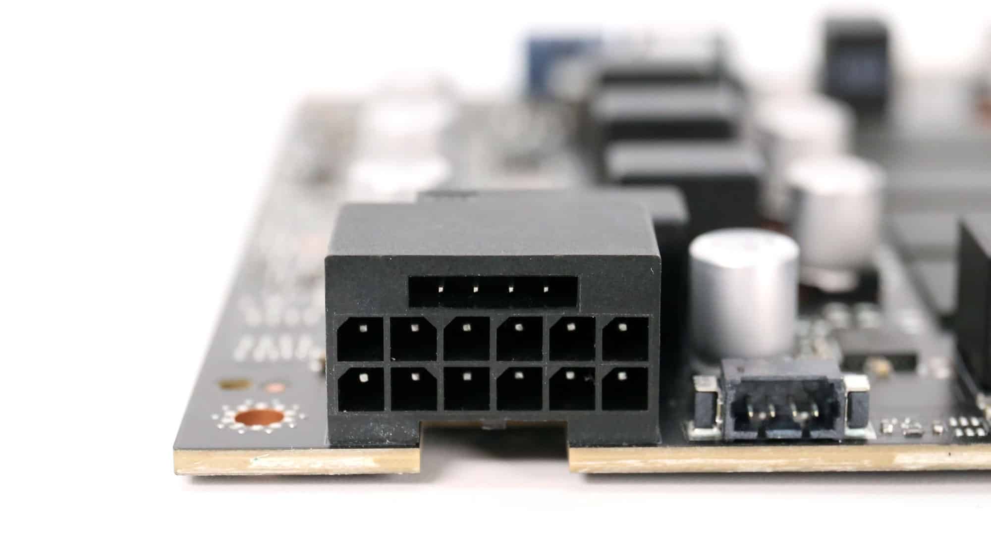
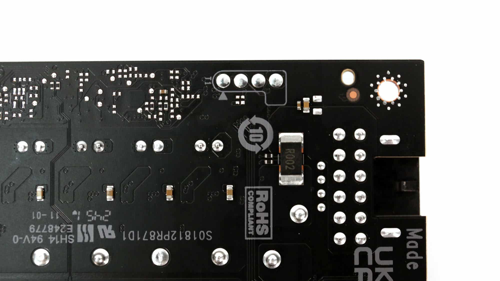
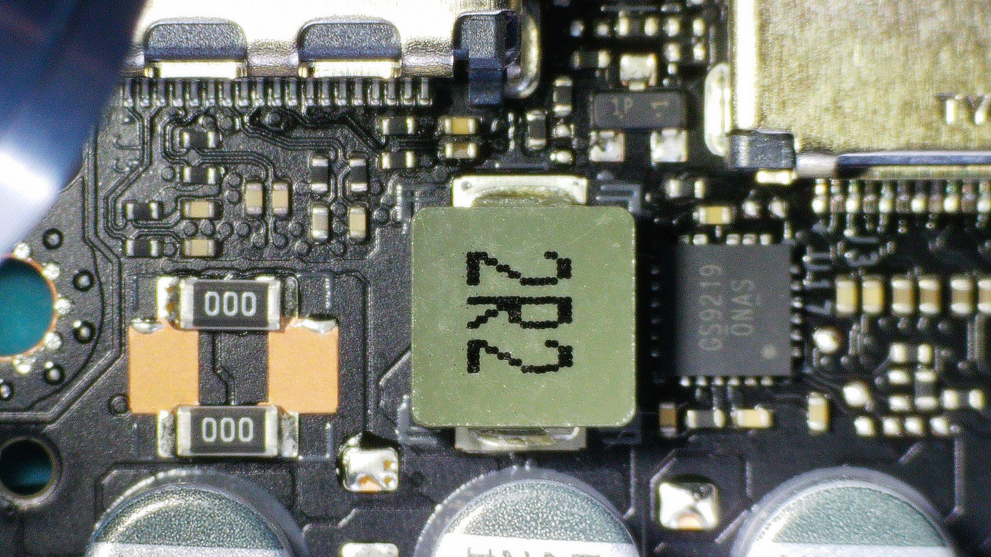
The card’s power socket. Its type is 12V-2×6.
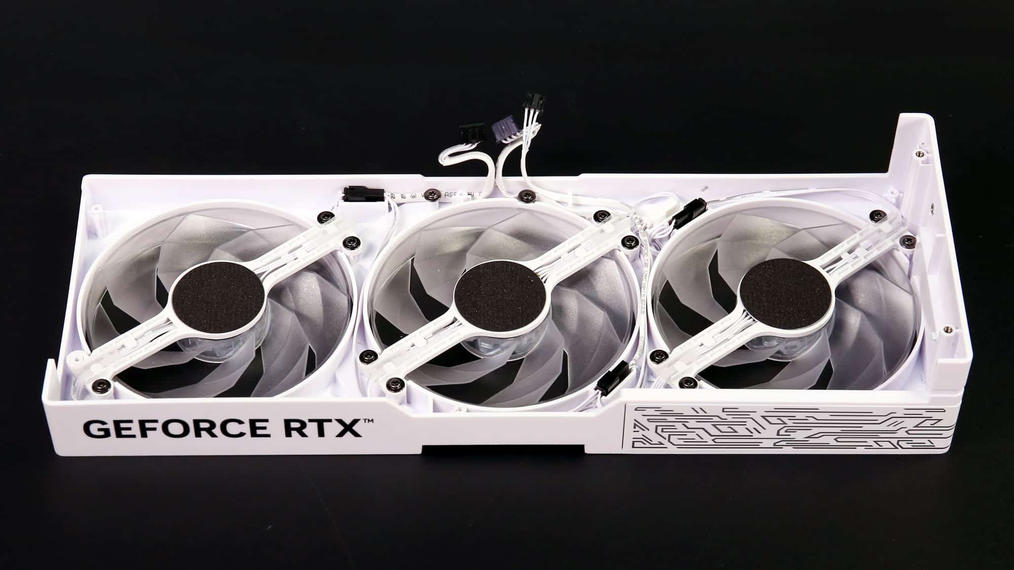
Photo provided by the Galax RTX 5080
There is no information on the fan model numbers, but they most likely use rifle bearings, like the rest of the fans Galax uses in its GPUs.
Some more photos of parts.
- Prologue & Technical specifications
- NVIDIA’s Key Technologies
- Box & Contents
- Part Analysis
- Specifications Comparison
- Test System
- Game Benchmark Details
- Raster Performance
- RT Performance
- RT Performance + DLSS/FSR Balanced
- Raytracing Performance + DLSS/FSR Balanced + FG
- DLSS/FSR Balanced (No RT)
- DLSS/FSR Balanced + FG (No RT)
- Relative Perf & Perf Per Watt (Raster)
- Relative Perf & Perf Per Watt (Raster + DLSS/FSR)
- Relative Perf & Perf Per Watt (RT)
- Relative Perf & Perf Per Watt (RT + DLSS/FSR)
- Relative Perf & Perf Per Watt (RT + DLSS/FSR + FG)
- Rendering Performance
- Operating Temperatures
- Operating Noise & Frequency Analysis
- Power Consumption
- Clock Speeds & Overclocking
- Cooling Performance
- Epilogue

Thanks for your detailed review. I bought a similar Galax card called the Blade OC in China. Despite putting it to the same settings as you in GPU tweak (and the GPU clock dial even going slightly higher to 2997) I’m finding that the max core clock I can get in TimeSpy Extreme GT1 is just under 3000MHz. Do you think this is just silicon lottery because my card seems to be about 3-5% behind every review of the Galax One click OC I can find (can’t read Chinese reviews of the local Blade OC version)?
Hi! OC is pure silicon lottery I am afraid.
OK. Cheers.