Part Analysis
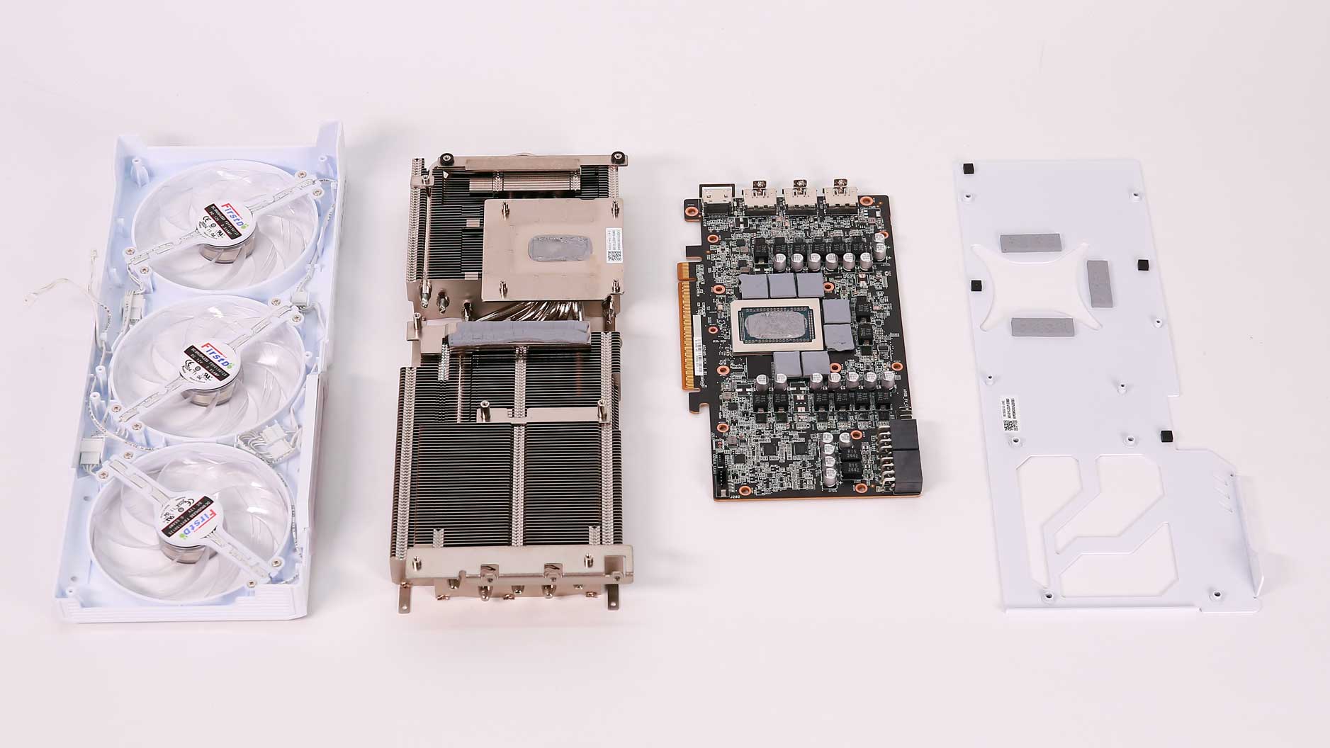
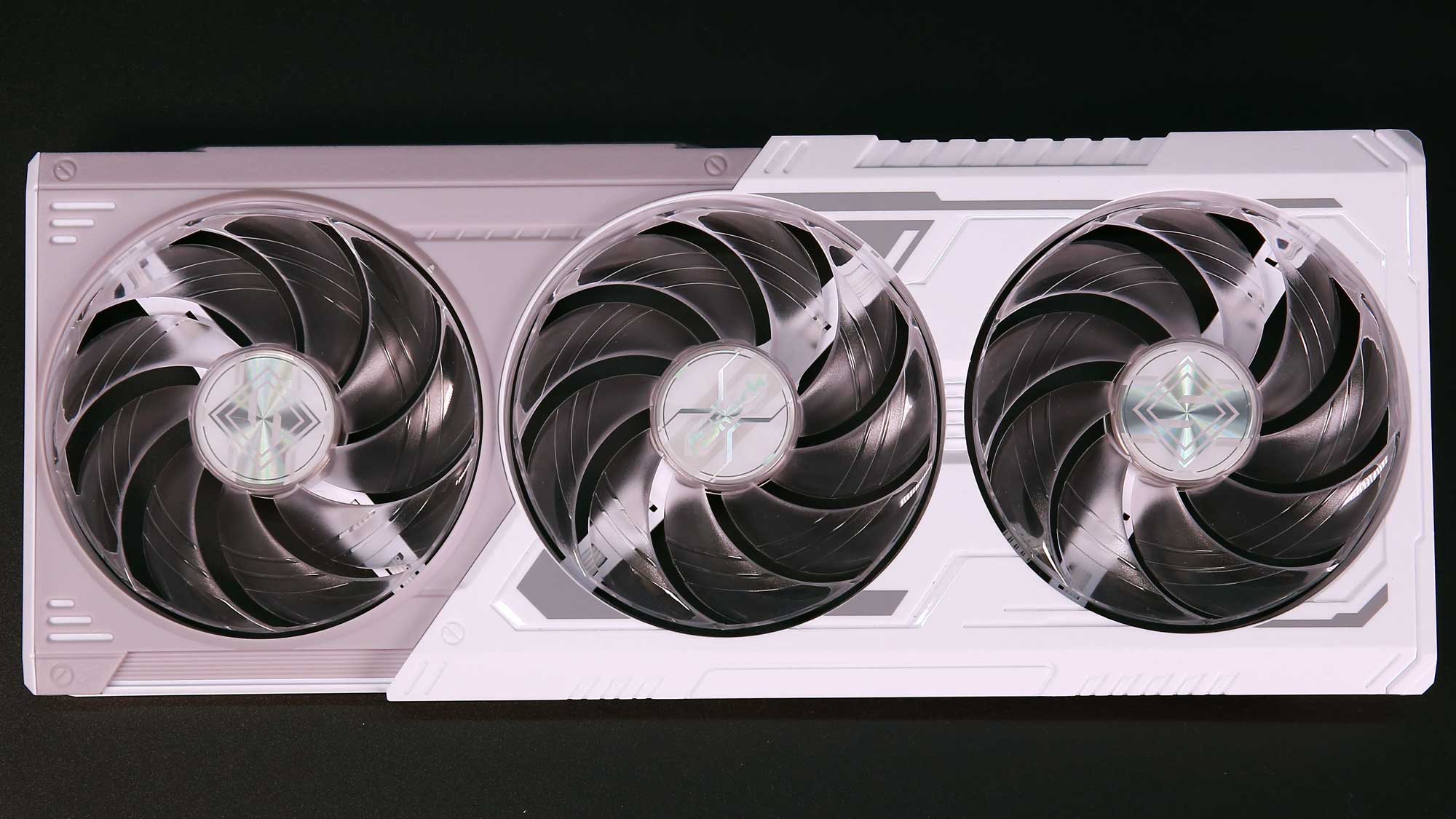
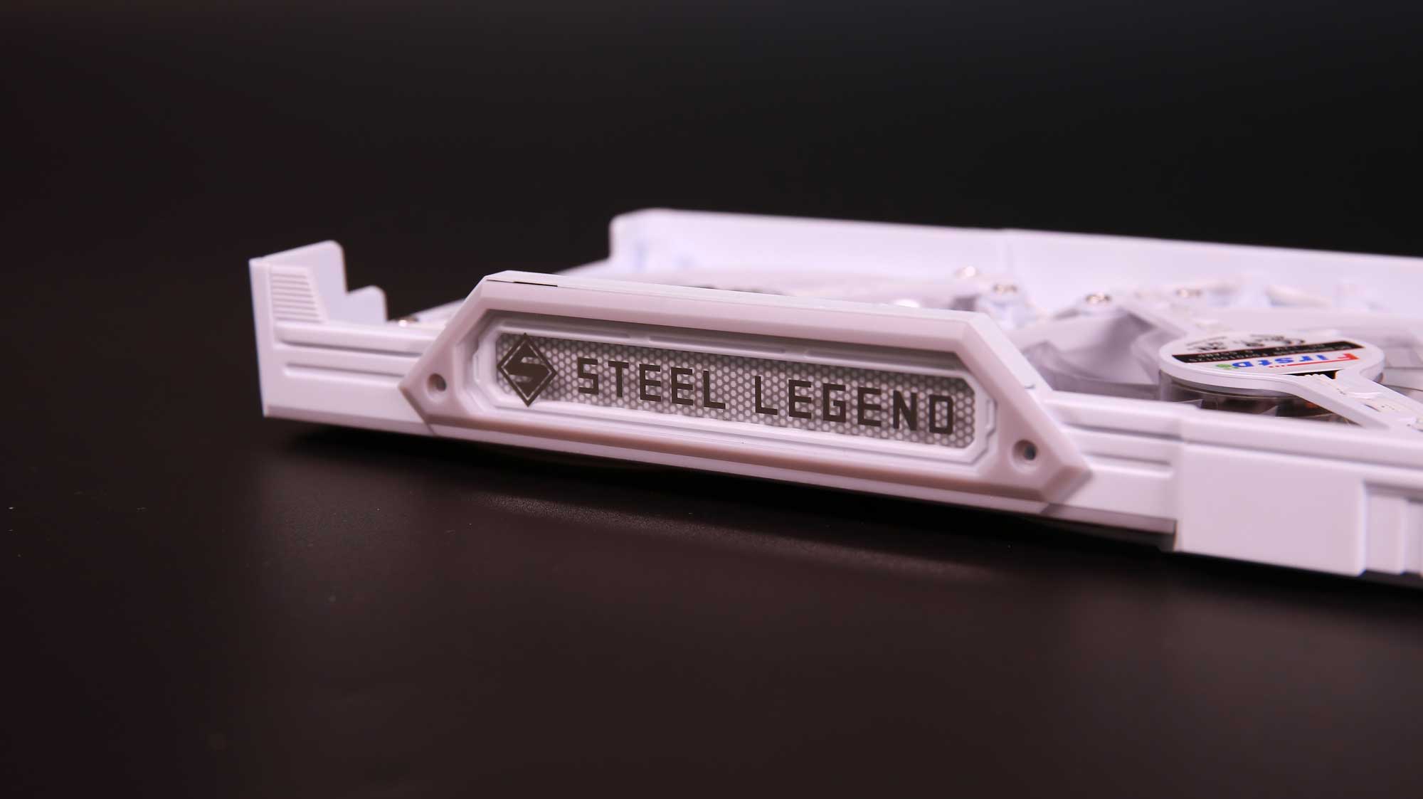
The main parts of the graphics card are the backplate, cooler, PCB, PCIe bracket, and fan assembly.
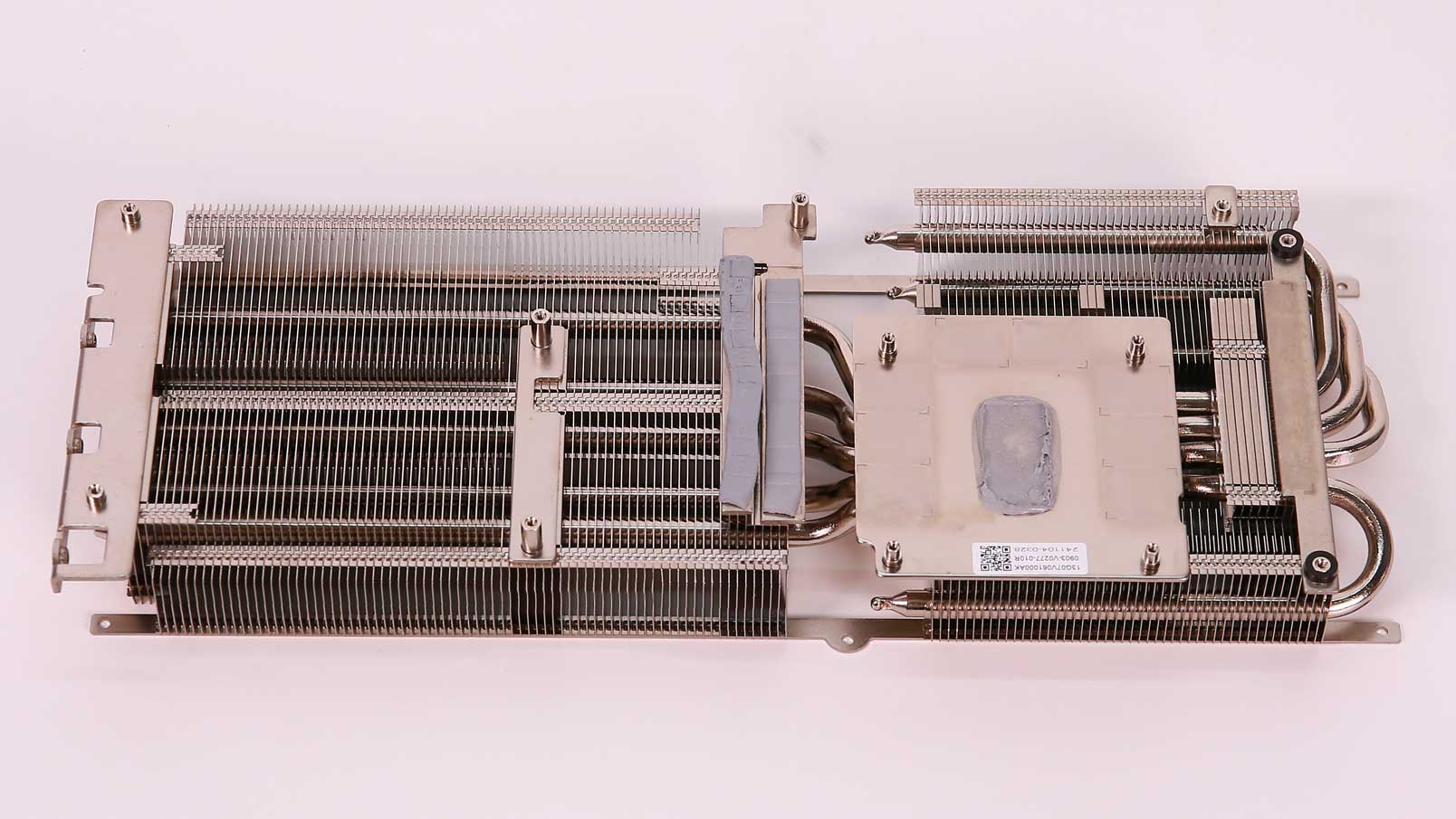
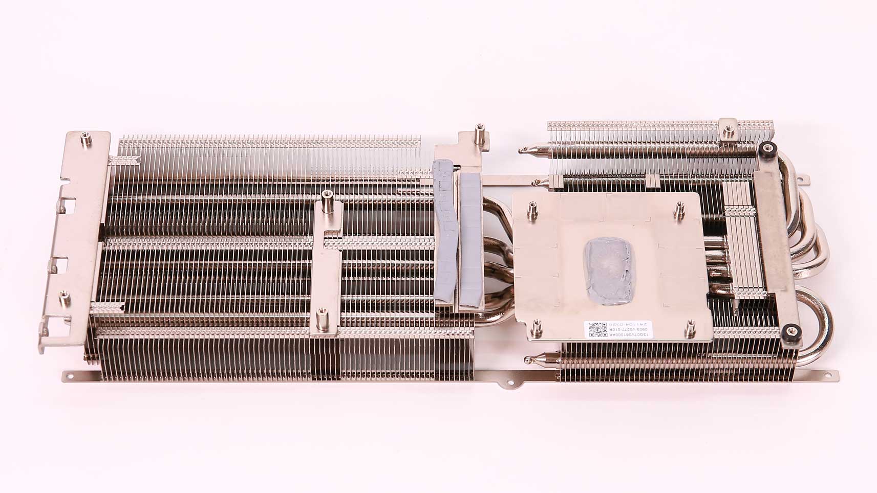
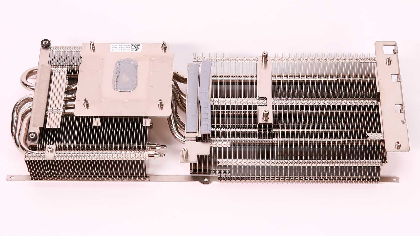
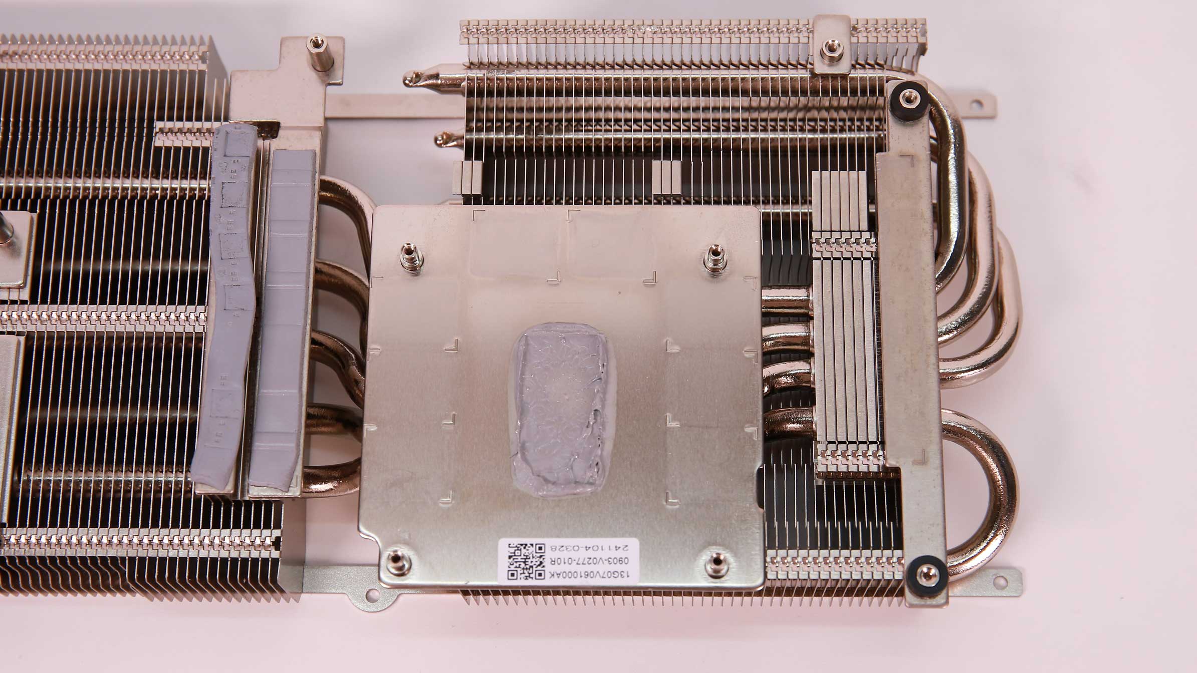
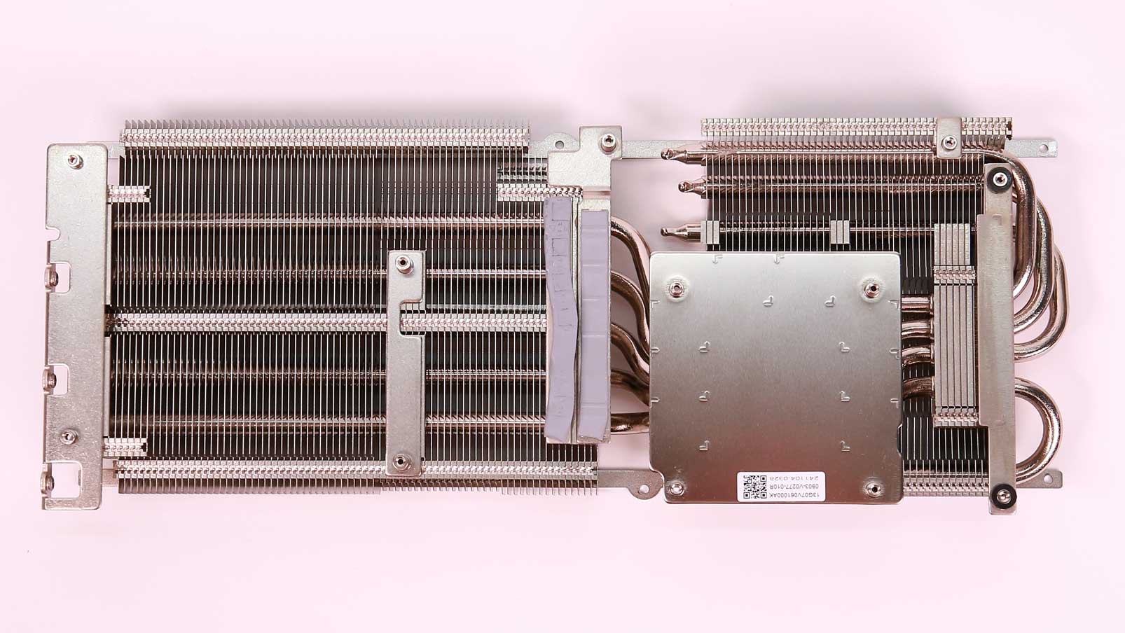
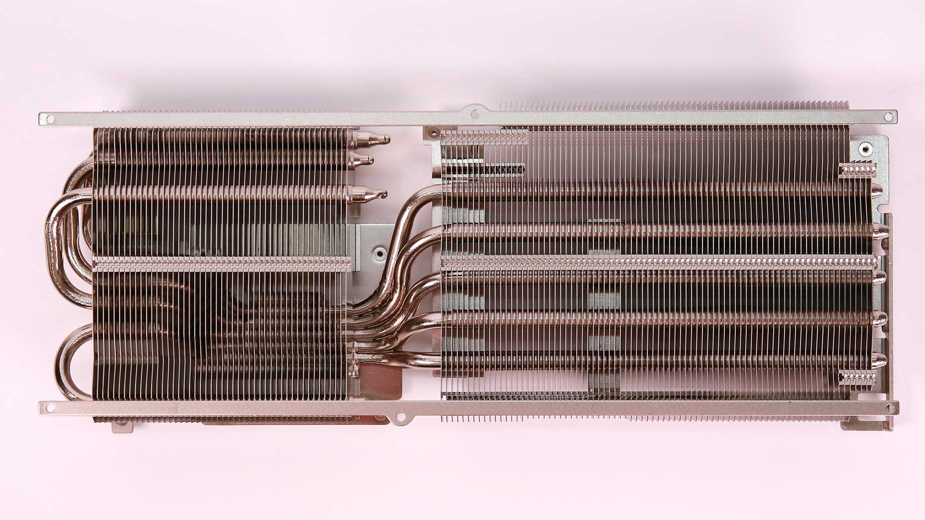
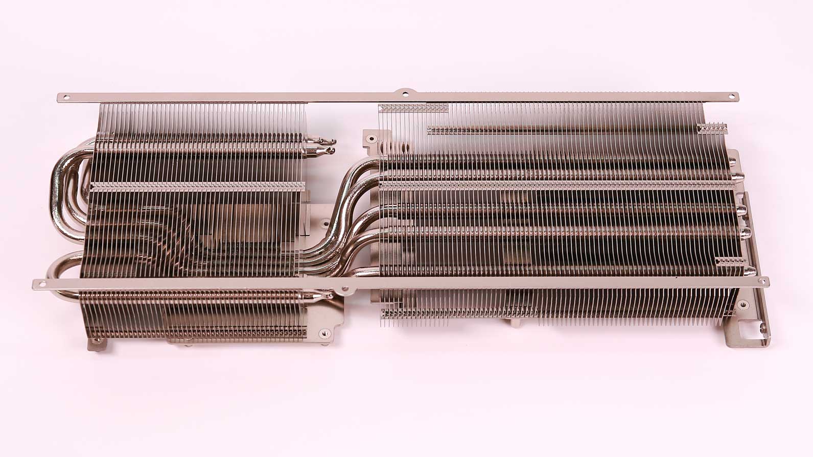
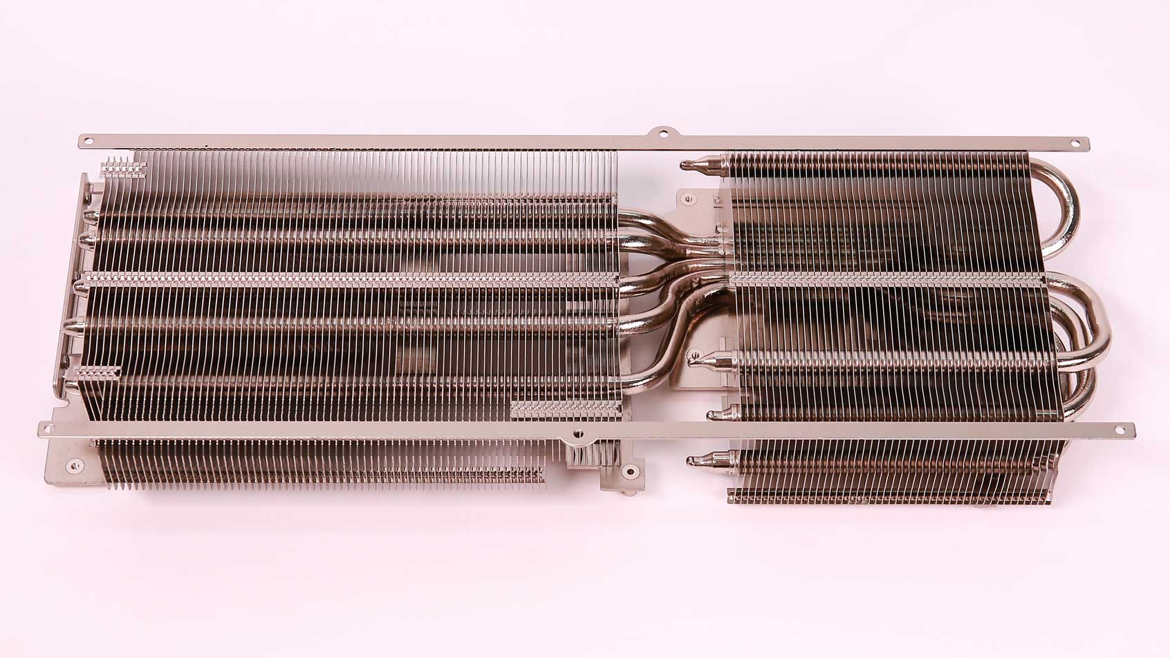
The cooling solution uses five heatpipes.
 |
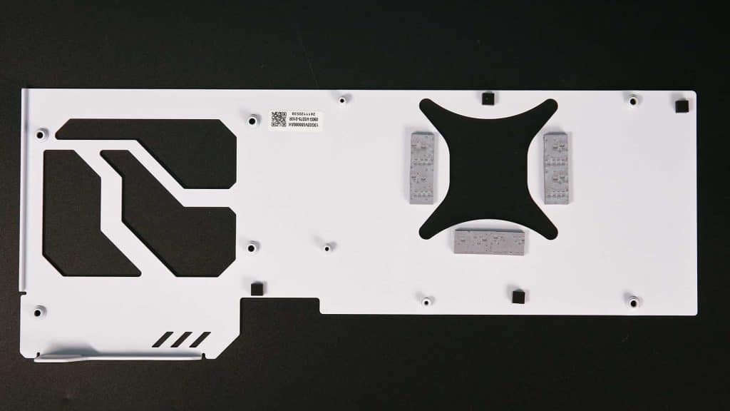 |
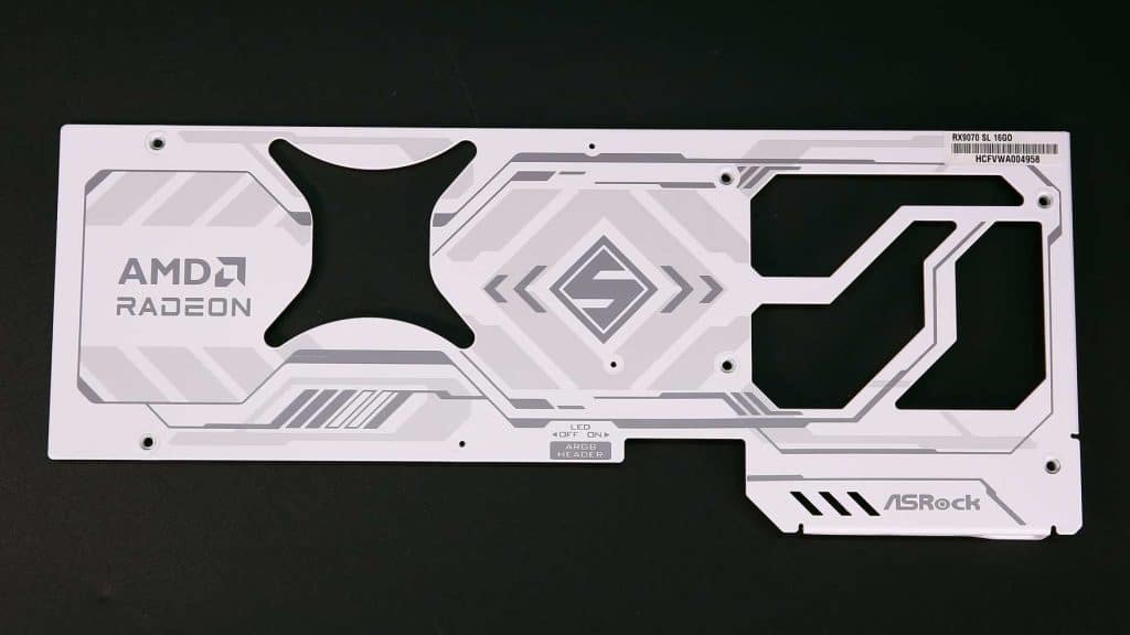
The backplate.
 |
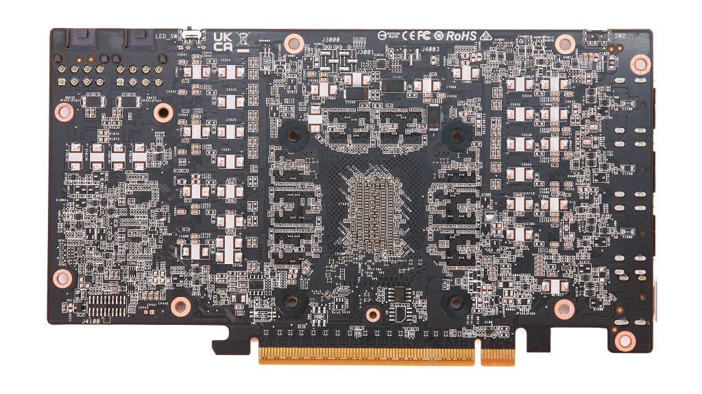 |
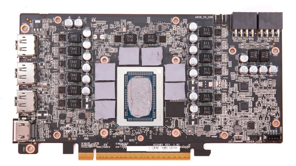
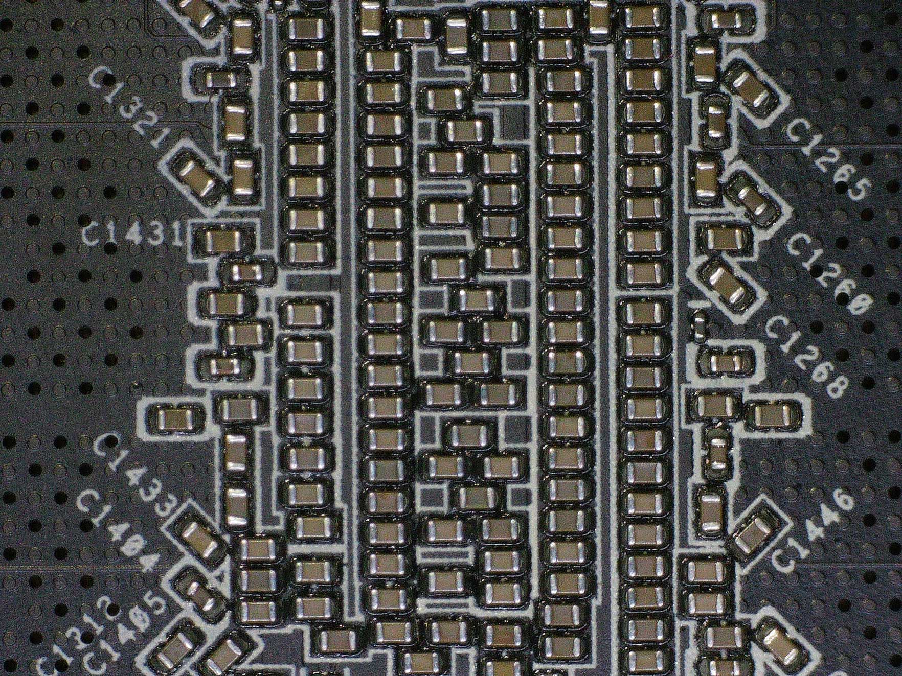
Here are photos of the PCB’s front and rear sides. It is sad to see most of the capacitor spots on the PCB’s back side empty. I wonder why ASRock didn’t bother installing them, and how they affect the GPU’s performance! On the top PCB side, Apaq provides all polymer caps.
![]()
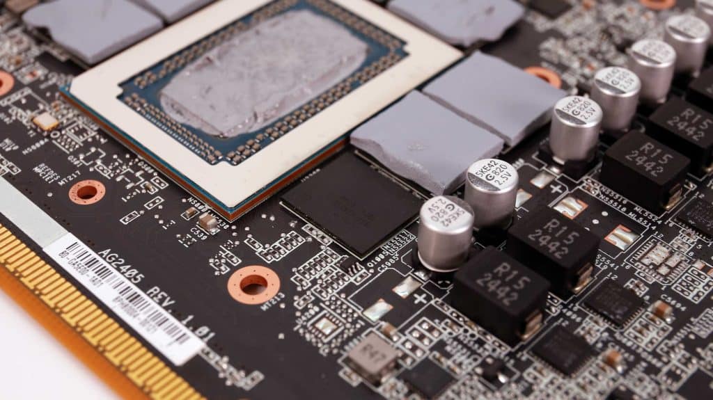
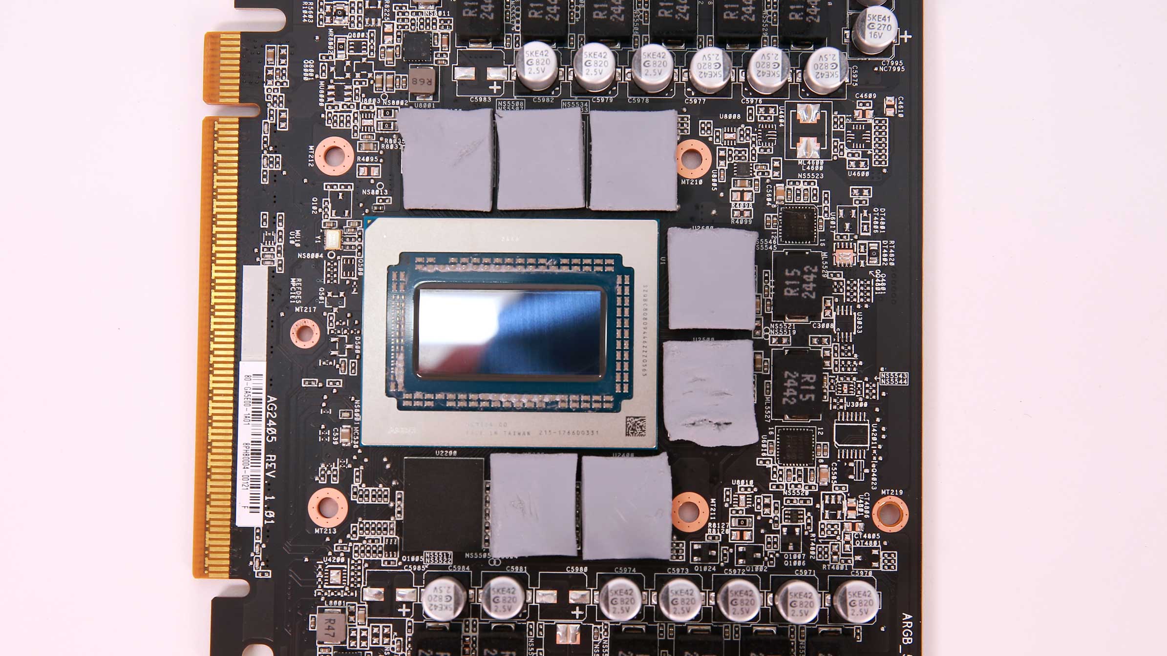
The AMD Navi 48 GPU follows the RDNA 4 architecture. TSMC manufactures it and uses a 5 nm production process. Its die size is 357 mm², and it has 53.9 billion transistors.
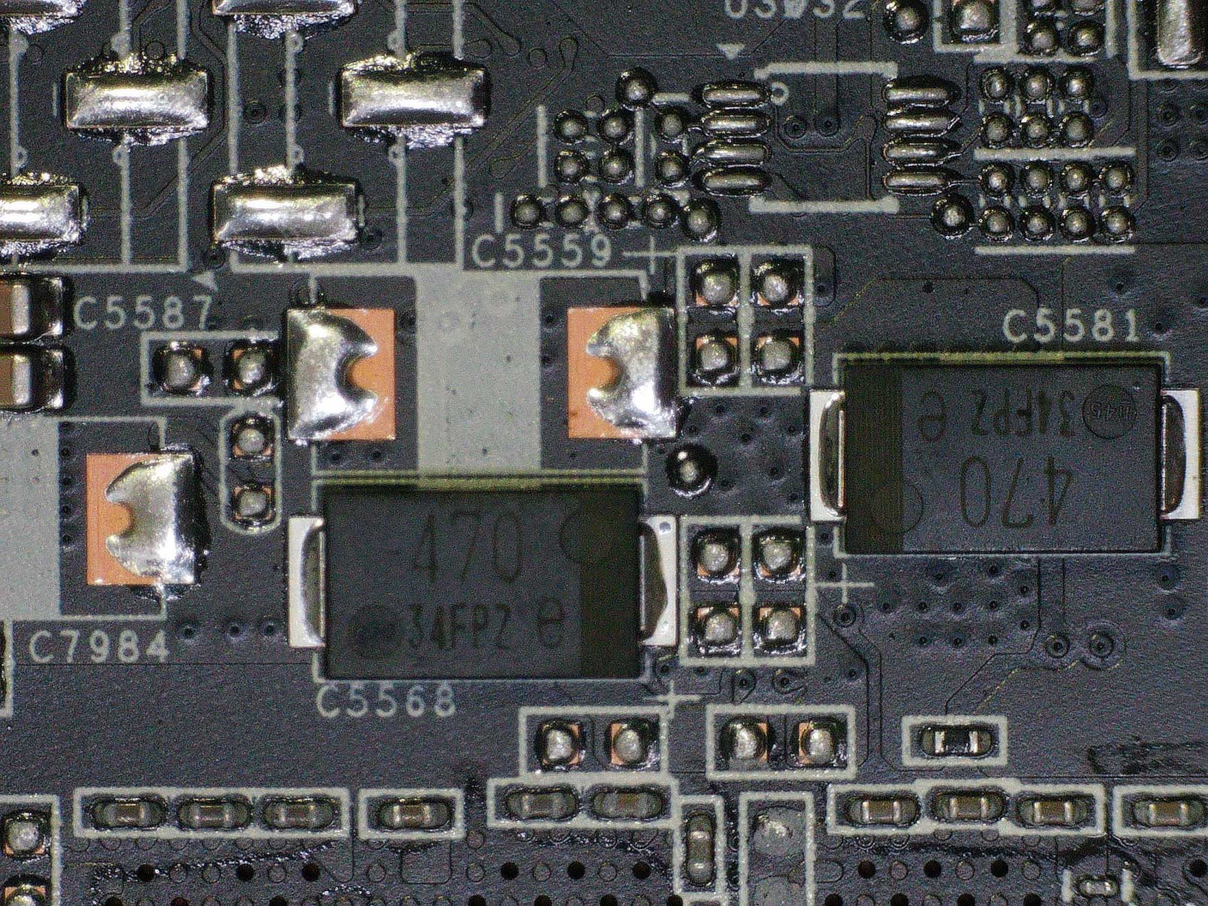
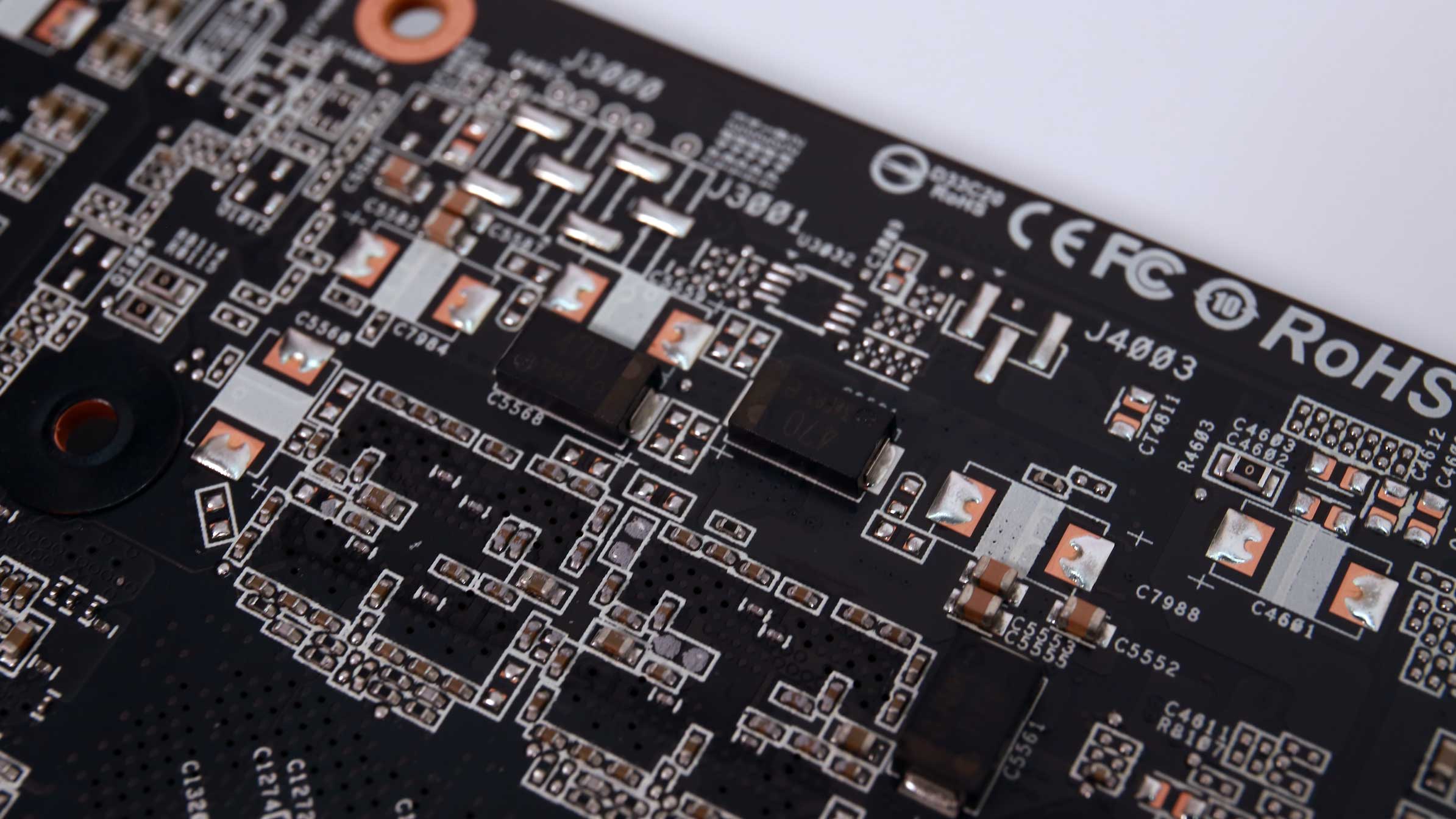
The capacitors behind the GPU provide power during the transient loads.
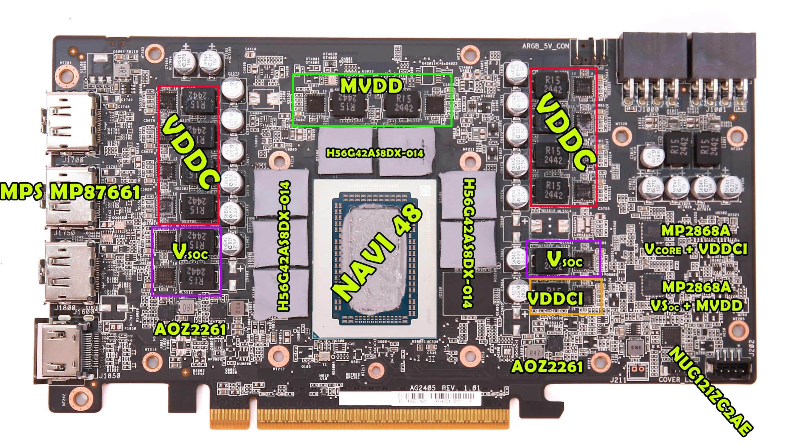
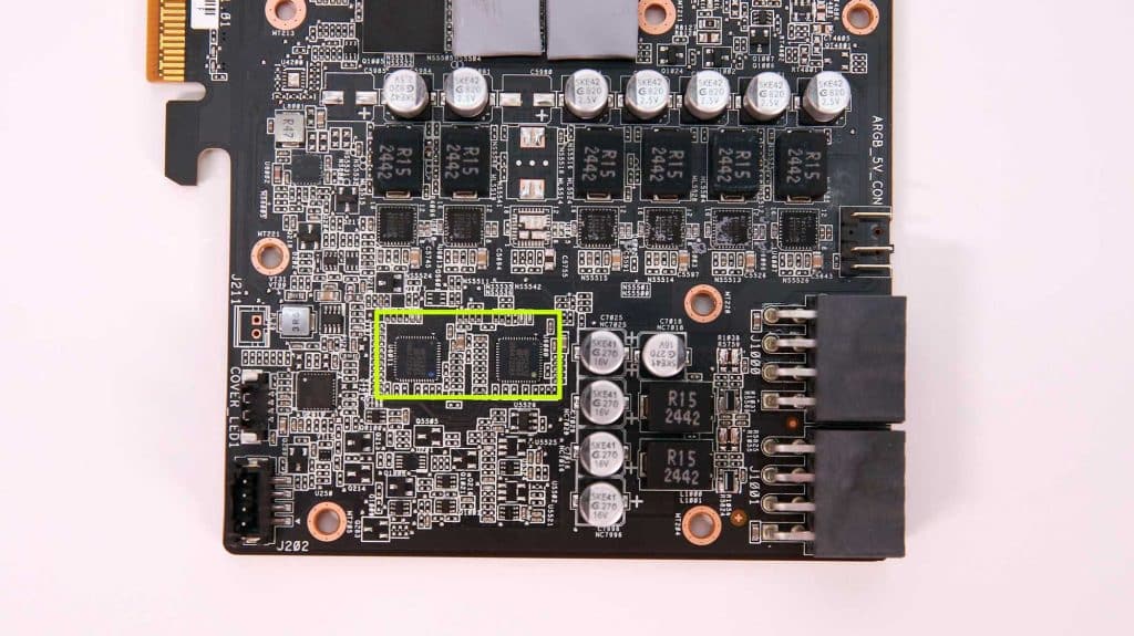
An 8+3-phase VRM (highlighted in red and purple) handles the GPU, and a 3-phase VRM (highlighted in green and orange) handles VRAM.
All power phases use
 |
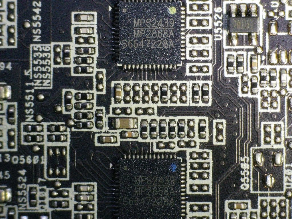 |
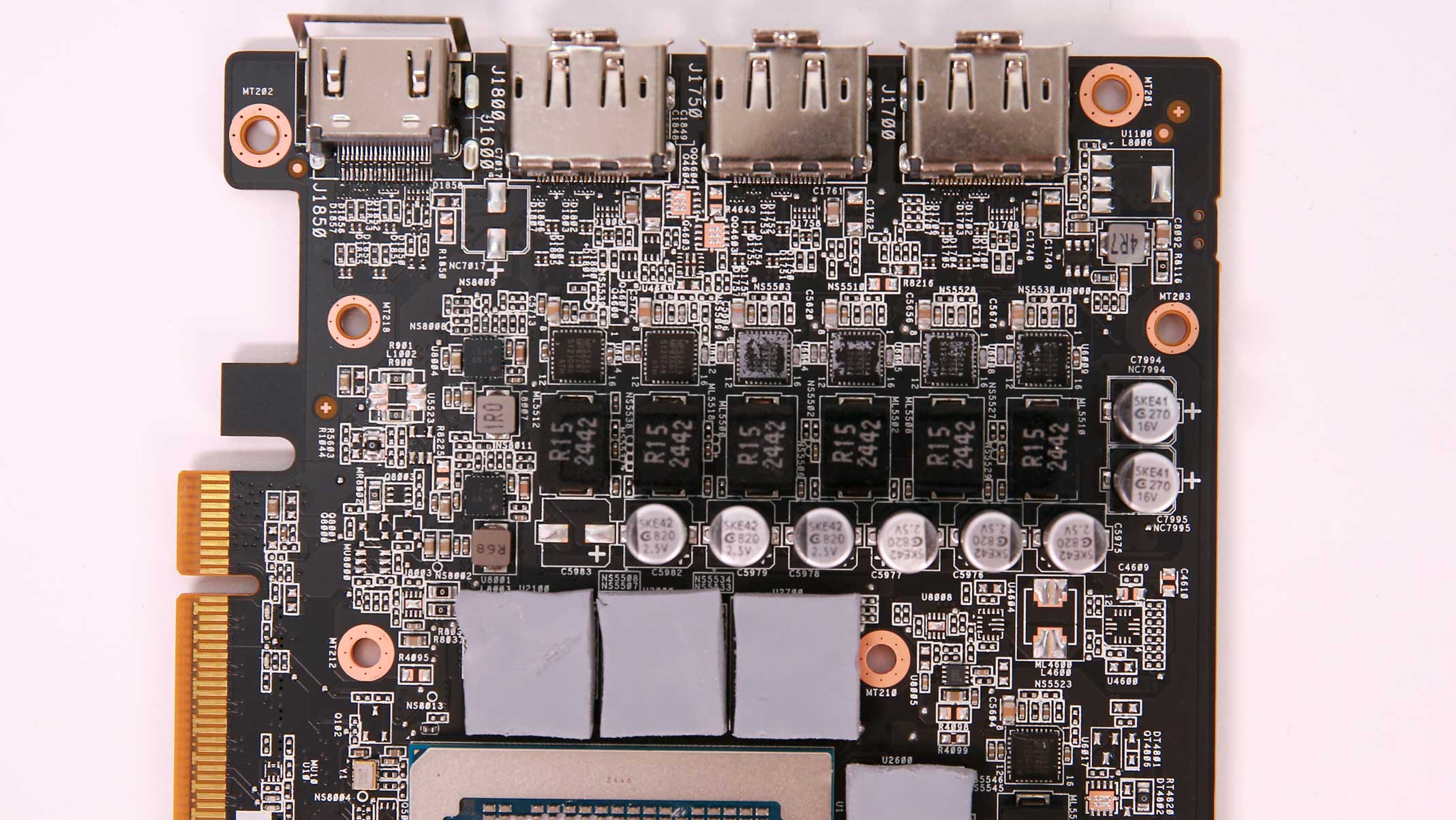
Two Monolithic Power Systems MP2868A controllers handle the board’s power phases for the GPU and its memory.
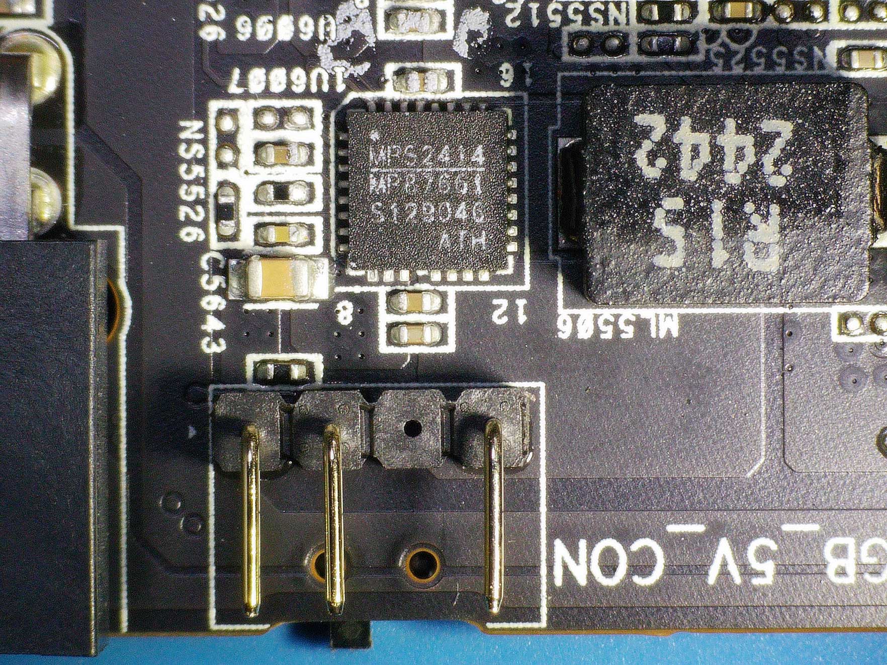
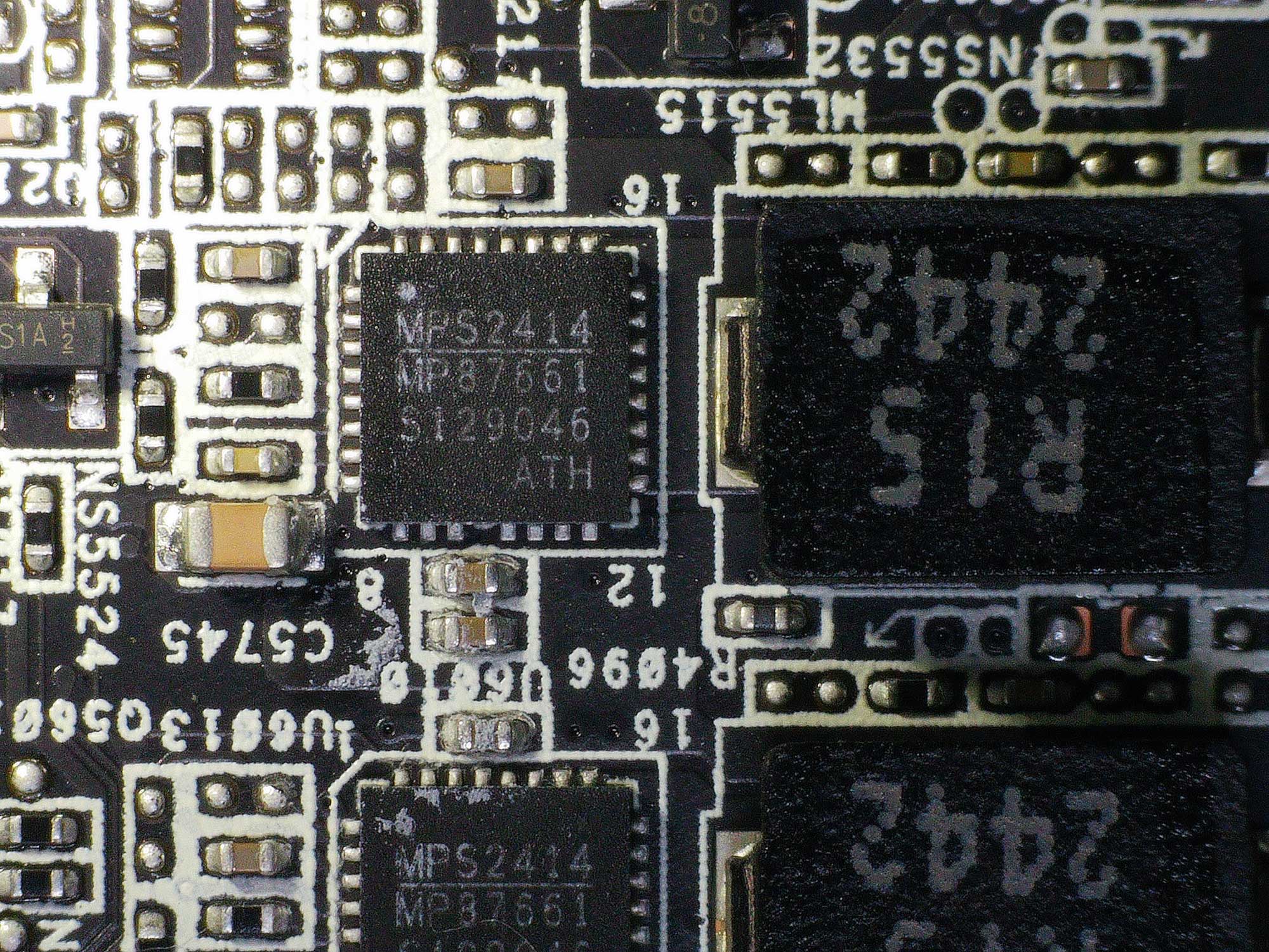
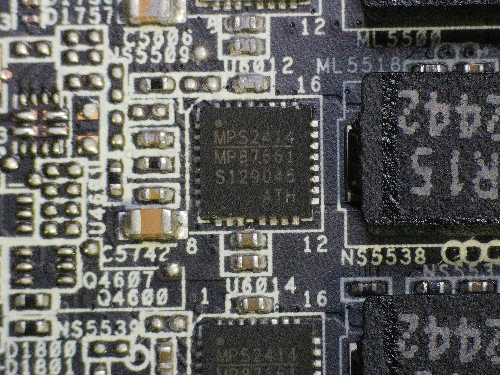
All GPU and VRAM VRM phases use Monolithic MPS MP87661 DrMOS with a rating of 60A.
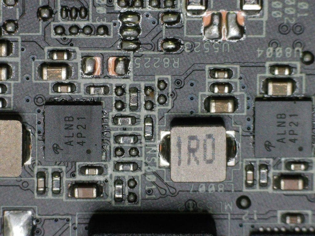
A pair of ALPHA OMEGA AOZ2261 synchronous buck regulators provides power to secondary circuits.
 |
 |
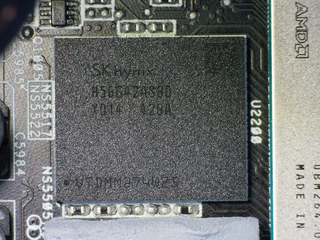
The H56G42AS8DX-014 GDDR6 memory chips are made by Hynix and are rated for 20 Gbps.
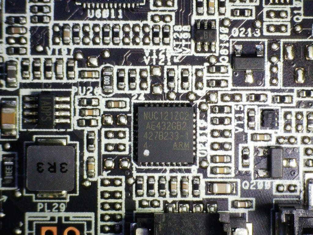
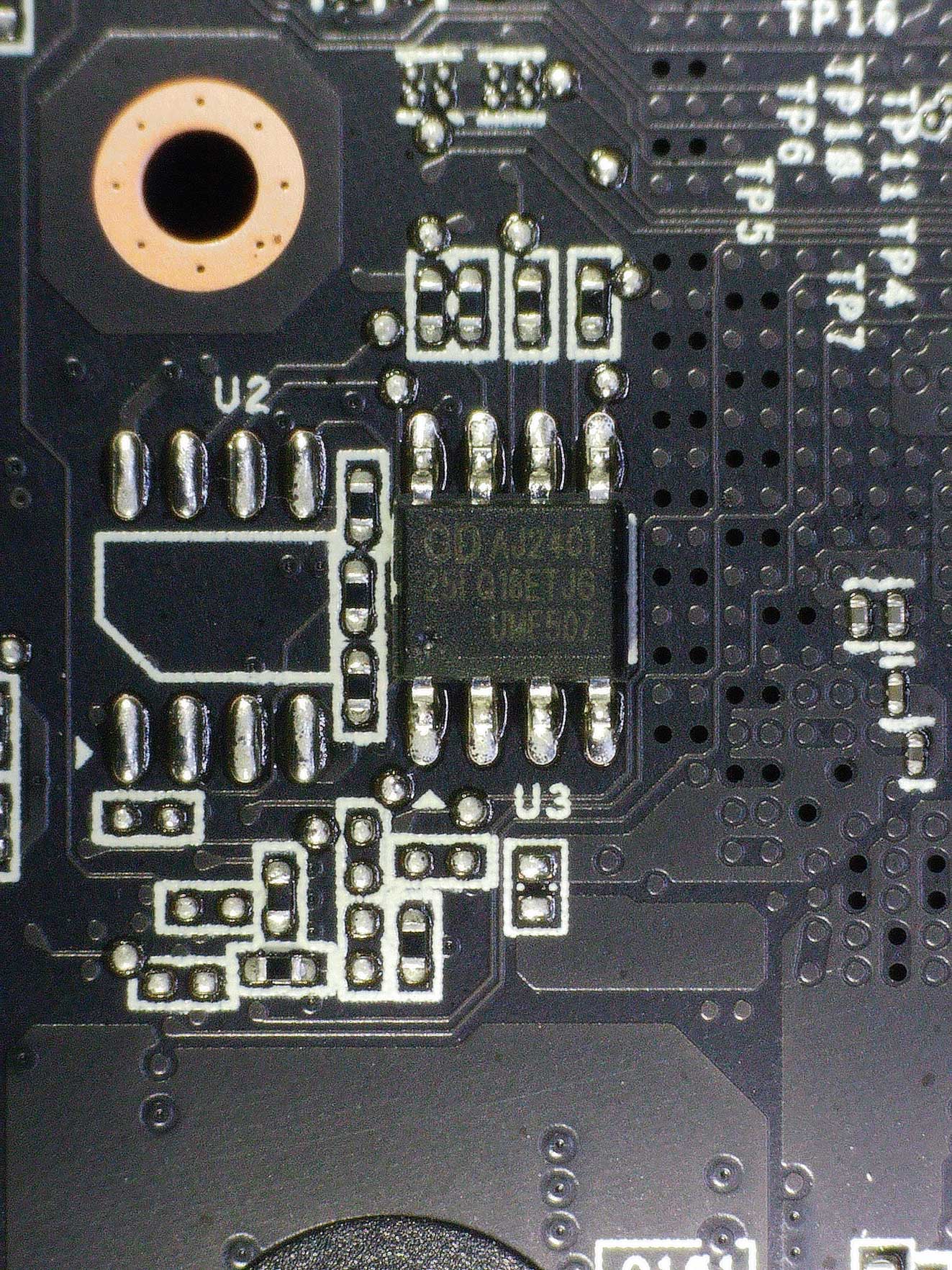
I found a NUC121ZC2AE 32-bit microcontroller ( MCU ) with ARM® Cortex-M0 core. It runs up to 50 MHz and supports 32 KB Flash, 8 KB SRA,M and 12-bit ADC.
 |
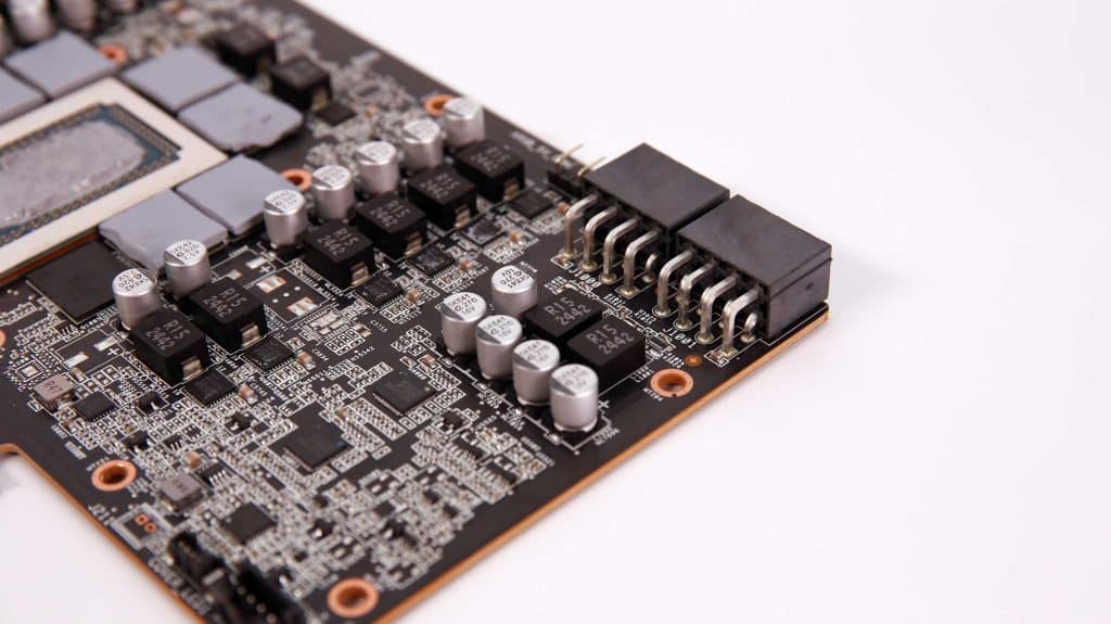 |
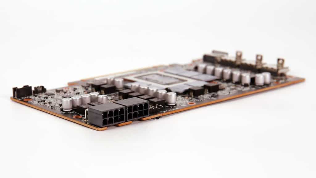
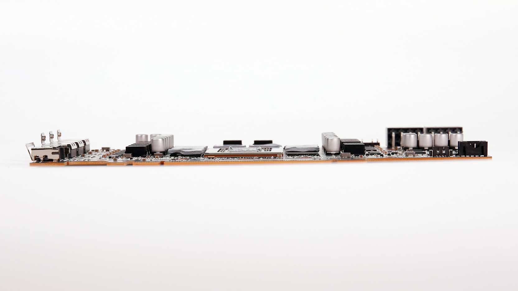
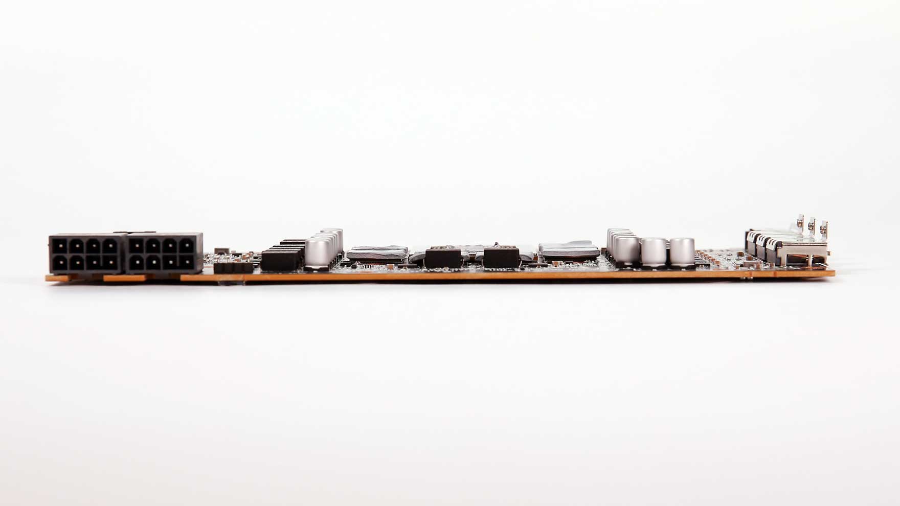
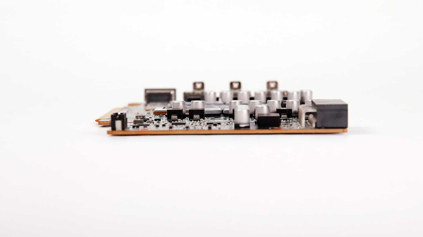
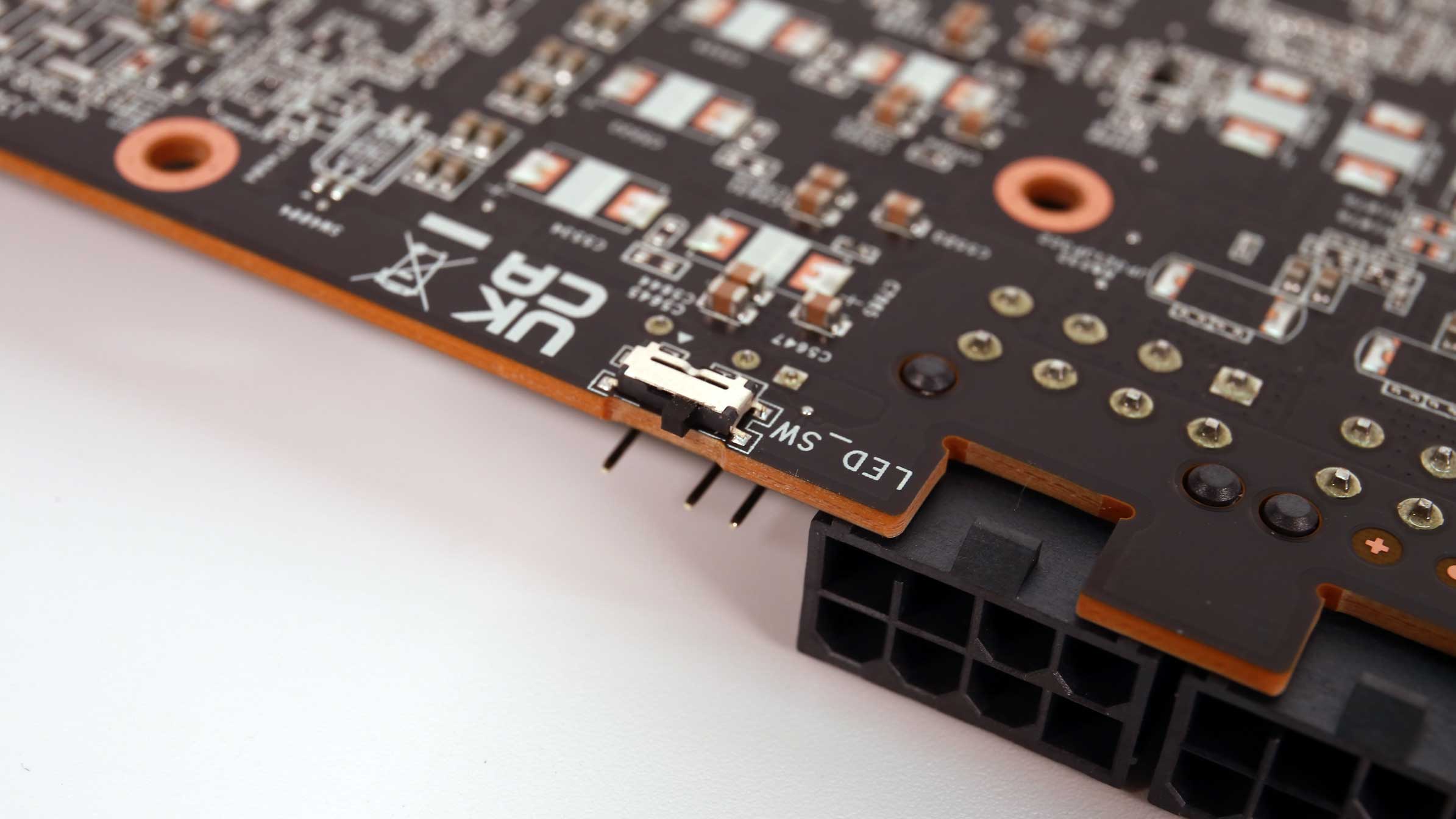
The card’s power sockets. Type PCIe 6+2 pin.
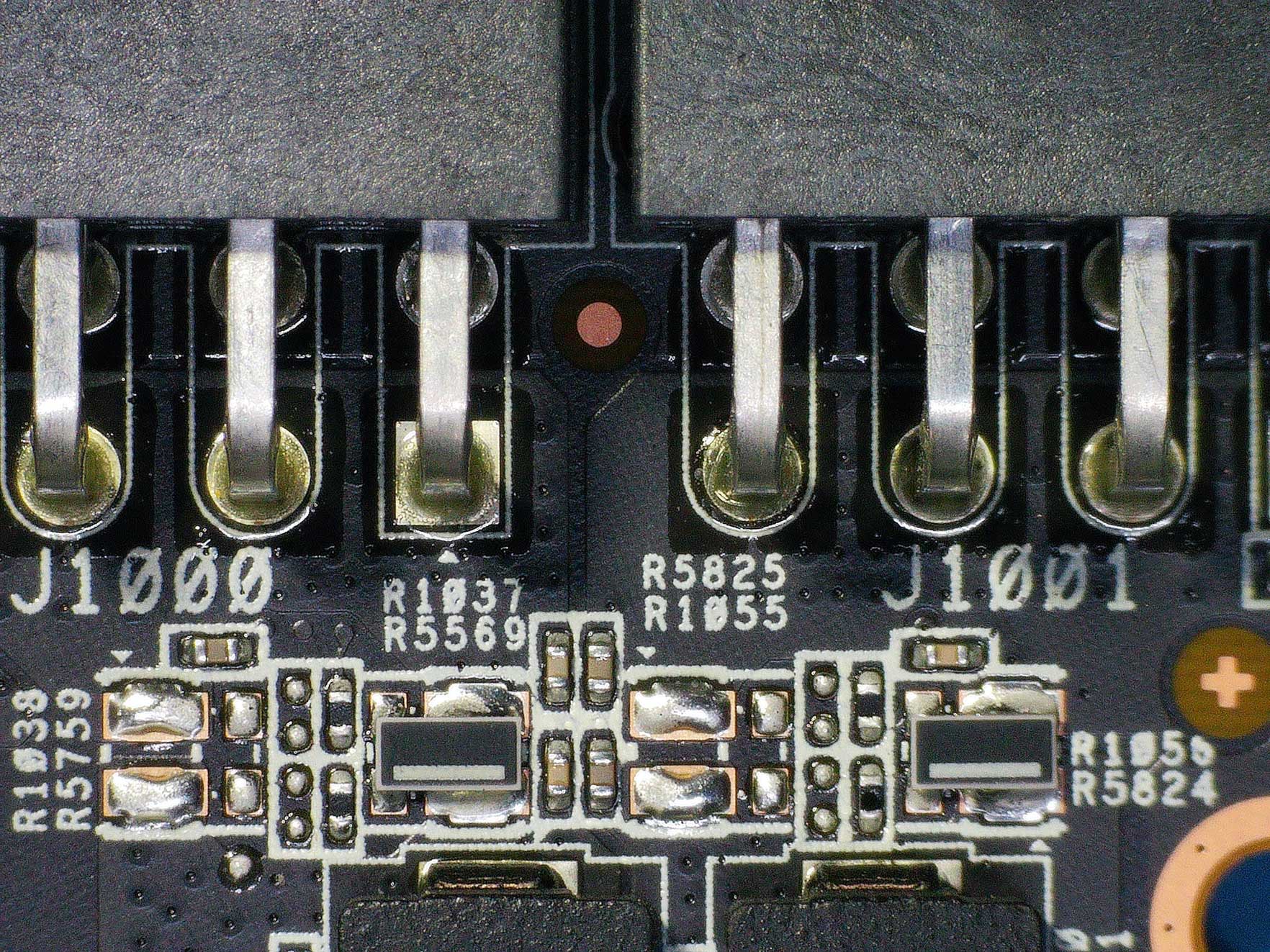
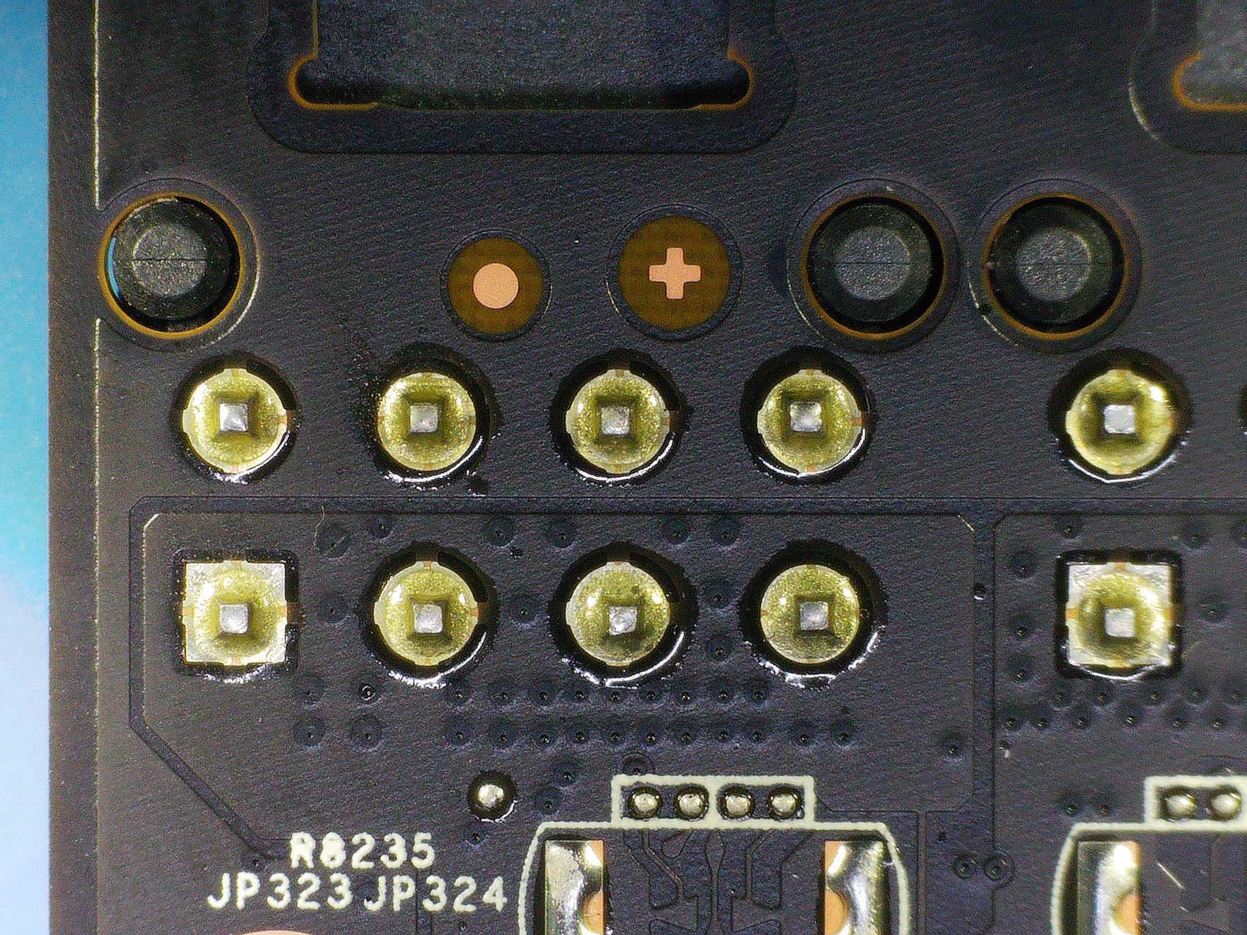
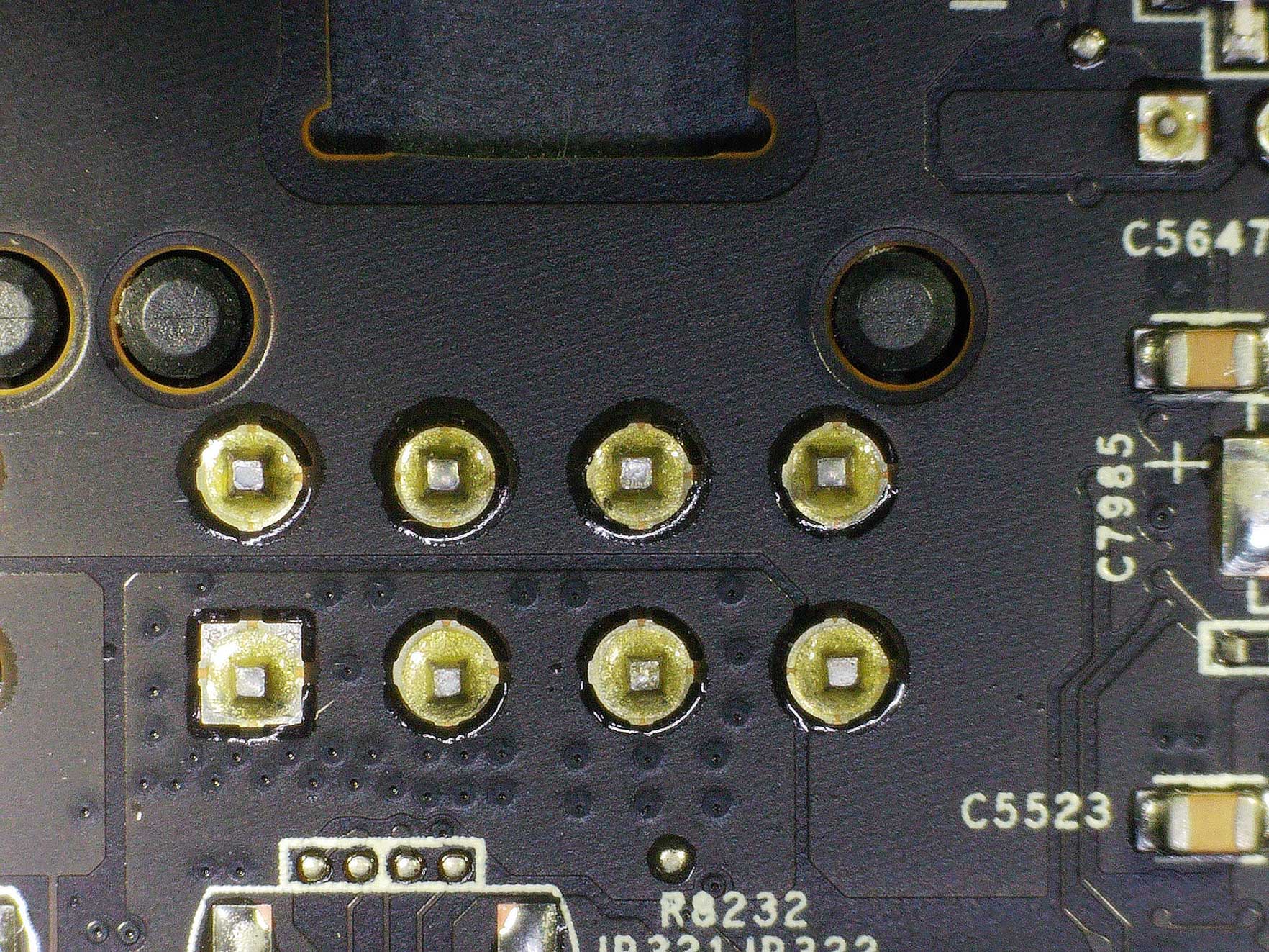
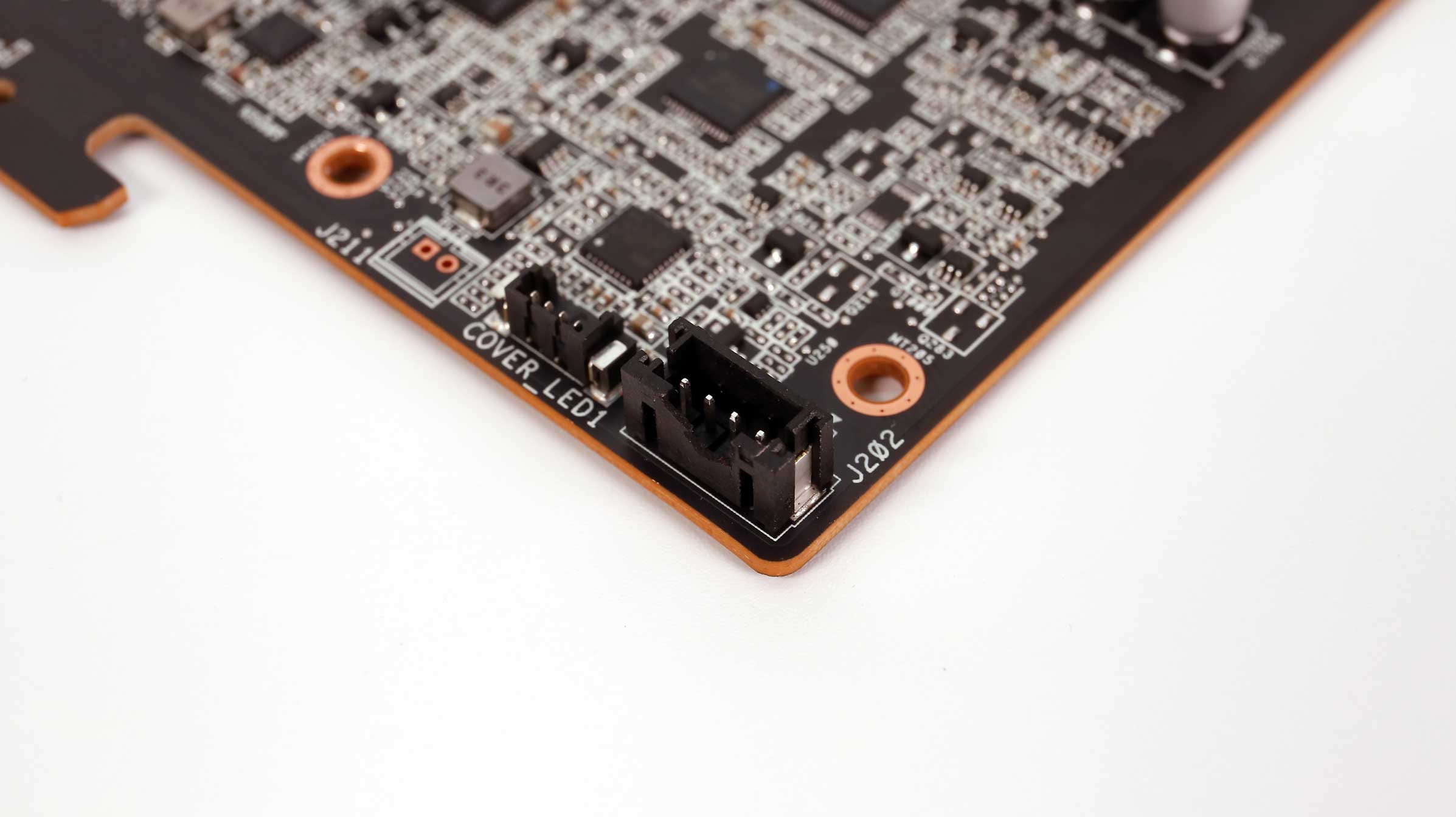
Some more photos of the board’s power headers.
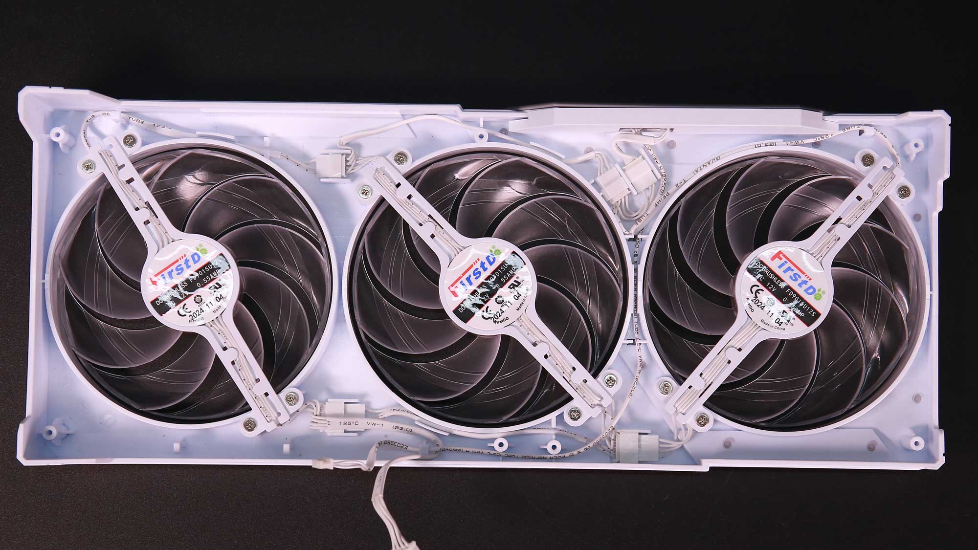
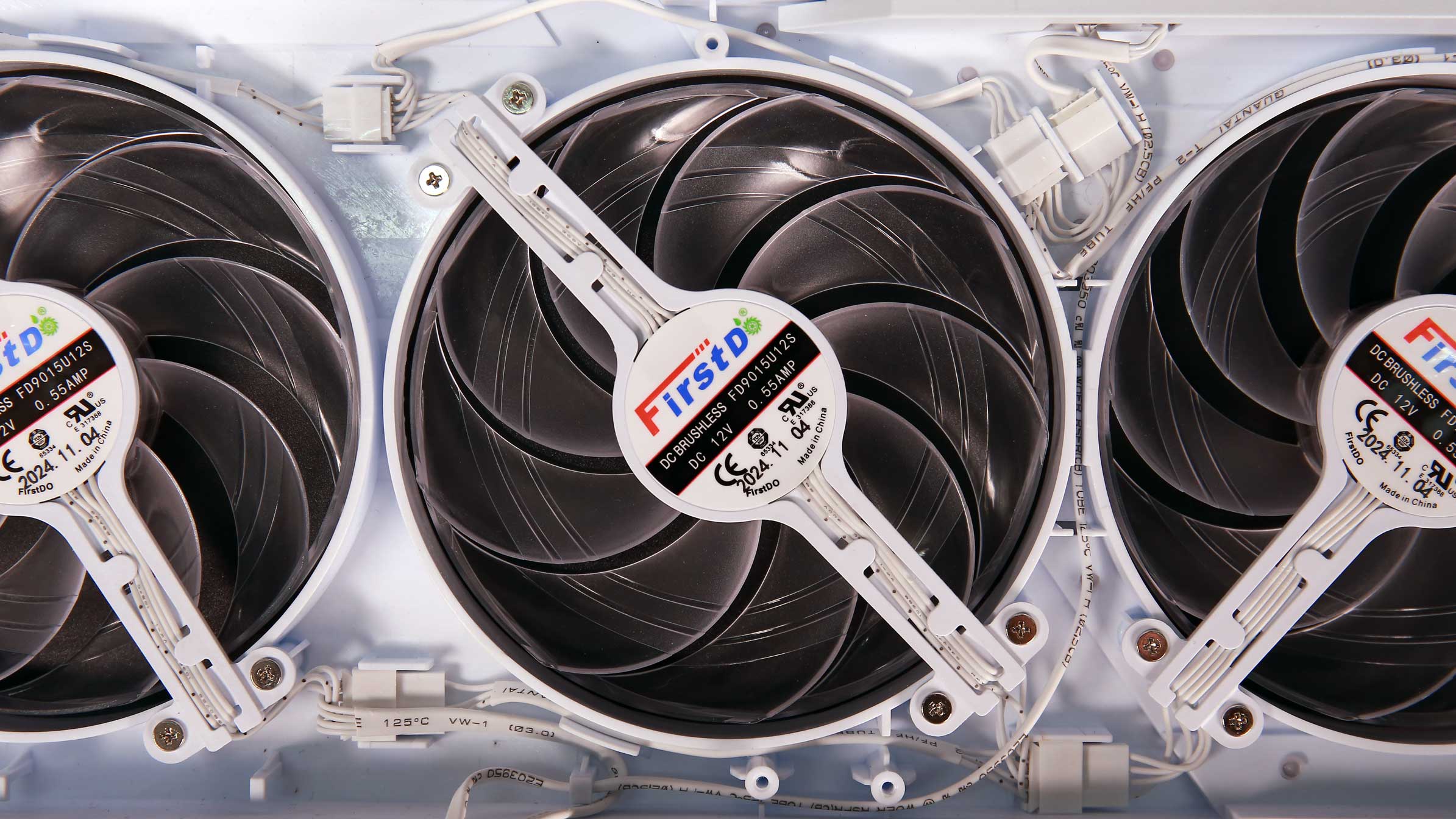
The fan’s model number is FD9015U12S. Its manufacturer is FirstD, a brand I have never heard of. I also don’t have a clue about their bearings, and I don’t want to destroy them to find this information.
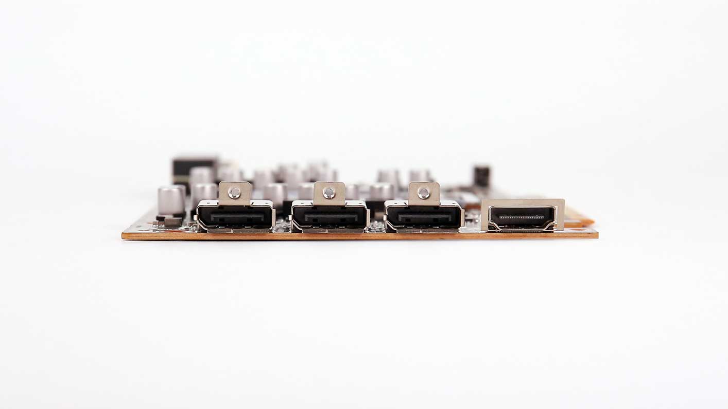
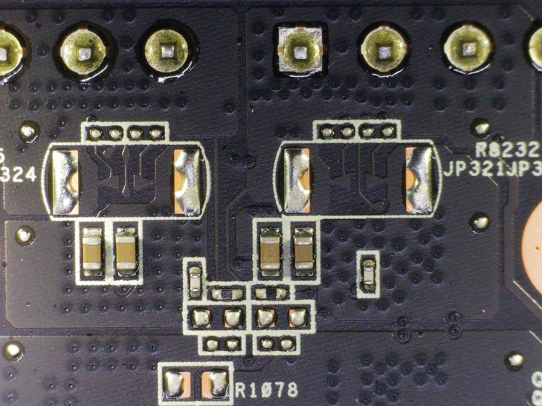
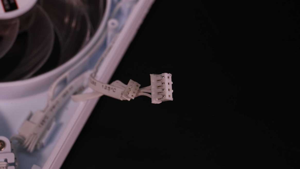
Some more photos of parts.
- Prologue & Technical specifications
- Ray Tracing Explained
- RDNA 4 Explained
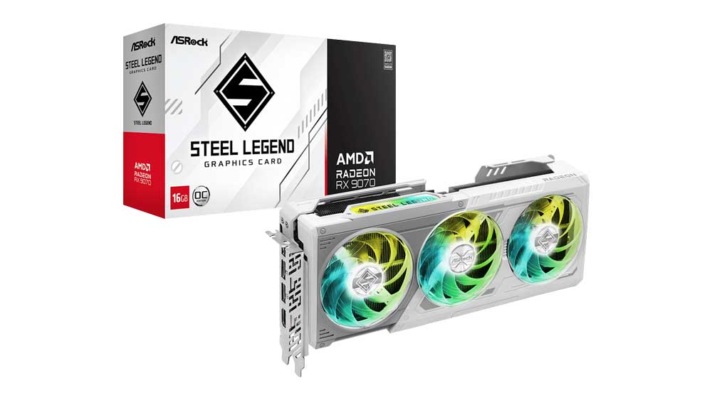
- Box & Contents
- Part Analysis
- Specifications Comparison
- Test System
- Game Benchmark Details
- Raster Performance
- RT Performance
- RT Performance + DLSS/FSR Balanced
- Raytracing Performance + DLSS/FSR Balanced + FG
- DLSS/FSR Balanced (No RT)
- DLSS/FSR Balanced + FG (No RT)
- Relative Perf & Perf Per Watt (Raster)
- Relative Perf & Perf Per Watt (Raster + DLSS/FSR)
- Relative Perf & Perf Per Watt (RT)
- Relative Perf & Perf Per Watt (RT + DLSS/FSR)
- Relative Perf & Perf Per Watt (RT + DLSS/FSR + FG)
- Rendering Performance
- Operating Temperatures
- Operating Noise & Frequency Analysis
- Power Consumption
- Clock Speeds & Overclocking
- Cooling Performance
- Epilogue

