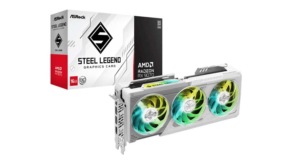
AMD’s RX 9070 series managed to disrupt the market, because of their decent prices, still notably higher than MSRP ones, and good performance. To put it midly, they were a pleasant suprise by AMD, and a tough opponent for NVIDIA’s RTX 5070 and 5070 Ti. In today’s review I will look at the ASRock Radeon RX 9070 Steel Legend model.
The AMD Radeon RX 9070 series consists of two members: the 9070 XT and the plain model. According to AMD, it sits between the RX 7900 XT(X) and RX 7900 GRE lines. The RX 9070 models have up to 64 CUs following the RDNA 4 architecture, and their GPUs consist of 53.9B transistors. The new GPUs are suitable for QHD and 4K gaming. The specs of both 9070 cards look similar, with the fundamental differences being on the CU units and the TDP. So, the 9070 XT has 64 CUs and 304W TDP, while the 9070 has 56 CUs and 220W TDP.
The 9070 series utilizes the RDNA 4 architecture, which includes updated ray tracing and AI accelerators. Combined with the 16GB of VRAM, these accelerators offer strong gaming performance. To improve ray tracing performance, AMD doubled the ray intersection rate. The ray intersection rate is the speed at which a system calculates how many rays intersect with objects in a 3D scene during ray tracing. AMD also used 2x ray accelerators per CU to handle all required calculations quickly and efficiently. According to AMD, the updated RT engine “doubles the performance for both ray-box and ray-triangle testing” compared to RDNA 3. Moreover, the RT engine uses 128KB of shared memory, which might look small, but it is okay for this operation.
Furthermore, AMD moved to BVH8, a type of Bounding Volume Hierarchy (BVH) used in ray tracing. It organizes objects in a scene into 8-node groups for faster ray intersection tests, improving performance by reducing the number of calculations needed to find collisions or intersections. Lastly, to improve RT performance, AMD introduced oriented bounding boxes to reduce or eliminate false positives in ray-triangle and ray-box intersections and a dedicated ray transform block to help with transformation. A dedicated ray transform block is specialized hardware in GPUs designed to accelerate the transformation and manipulation of rays during ray tracing. It handles tasks like ray-object intersection calculations more efficiently, improving overall ray-tracing performance.
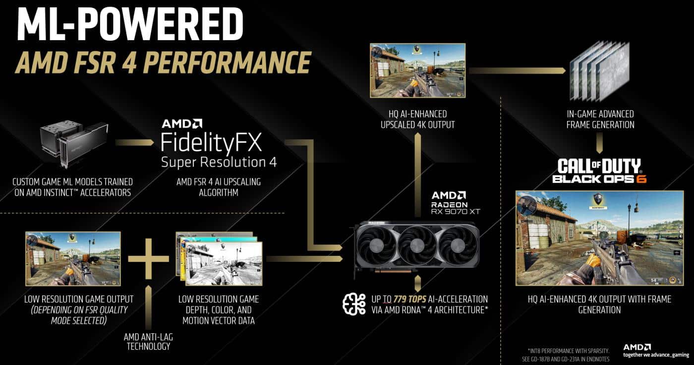
We shouldn’t forget AMD’s new software technologies, like FSR 4, an upscaling technology that transforms low-resolution frames into higher-fidelity ones, increasing performance. The FSR 4 upscaling algorithm now uses an advanced AI model, which exploits the RDNA AI accelerator for improved performance. However, we will talk more about FSR 4 on the next page.
The tables below show the specs of the RTX 50/40 series, AMD, and Intel models.
NVIDIA Graphics Cards Major Specs
RTX 50 Series
| RTX 5090 | RTX 5080 | RTX 5070 Ti | RTX 5070 | |
| Architecture | GB202 | GB203 | GB203 | GB205 |
| Process Technology | TSMC 4N | TSMC 4N | TSMC 4N | TSMC 4N |
| Base Clock (MHz) | 2010 | 2300 | 2300 | 2160 |
| Boost Clock (MHz) | 2410 | 2620 | 2450 | 2510 |
| VRAM Size (GB) | 32 | 16 | 16 | 12 |
| VRAM Type | GDDR7 | GDDR7 | GDDR7 | GDDR7 |
| VRAM Speed (Gbps) | 28 | 30 | 28 | 28 |
| VRAM Bus Width (bit) | 512 | 256 | 256 | 192 |
| Transistors (Billions) | 92.2 | 45.6 | 45.6 | 31.0 |
| Shading Units | 21760 | 10752 | 8960 | 6144 |
| TMUs/Tensor Cores | 680 | 336 | 280 | 192 |
| ROPs | 176 | 128 | 96 | 64 |
| SM/RT Cores | 170 | 84 | 40 | 48 |
| TDP (W) | 575 | 360 | 300 | 250 |
| Launch Month/Year | 1/2025 | 1/2025 | 1/2025 | 1/2025 |
| MSRP ($) | 2000 | 1000 | 750 | 550 |
RTX 40 Series
| RTX 4090 | RTX 4080 Super | RTX 4070 Ti Super | RTX 4070 Super | RTX 4070 | RTX 4060 Ti | |
| Architecture | AD102 | AD103 | AD103 | AD104 | AD104 | AD106 |
| Process Technology | TSMC 5N | TSMC 5N | TSMC 5N | TSMC 5N | TSMC 5N | TSMC 5N |
| Base Clock (MHz) | 2235 | 2295 | 2340 | 1980 | 1920 | 2310 |
| Boost Clock (MHz) | 2520 | 2550 | 2610 | 2475 | 2475 | 2535 |
| VRAM Size (GB) | 24 | 16 | 16 | 12 | 12 | 8 |
| VRAM Type | GDDR6X | GDDR6X | GDDR6X | GDDR6X | GDDR6X | GDDR6 |
| VRAM Speed (Gbps) | 21 | 23 | 21 | 21 | 21 | 18 |
| VRAM Bus Width (bit) | 384 | 256 | 256 | 192 | 192 | 128 |
| Transistors (Billions) | 76.3 | 45.9 | 45.9 | 35.8 | 35.8 | 22.9 |
| Shading Units | 16384 | 10240 | 8448 | 7168 | 5888 | 4352 |
| TMUs/Tensor Cores | 512 | 320 | 264 | 224 | 184 | 136 |
| ROPs | 176 | 112 | 96 | 80 | 64 | 48 |
| SM/RT Cores | 128 | 80 | 66 | 56 | 46 | 34 |
| TDP (W) | 450 | 320 | 285 | 220 | 200 | 160 |
| Launch Month/Year | 9/22 | 1/2024 | 1/24 | 1/24 | 4/23 | 4/23 |
| Street Price ($) | 2500 | 1600 | 915 | 640 | 570 | 399 |
The table below contains the specs of AMD’s current-generation graphics cards for reference purposes.
AMD Graphics Cards Major Specs
| RX 9070 XT | RX 9070 | RX 7900 XTX | RX 7900 XT | RX 7900 GRE | RX 7800 XT | RX 7700 XT | |
| Architecture | Navi 48 | Navi 48 | Navi 31 | Navi 31 | Navi 31 | Navi 32 | Navi 32 |
| Process Technology | TSMC N4 | TSMC N4 | TSMC N5/N6 | TSMC N5/N6 | TSMC N5/N6 | TSMC N5/N6 | TSMC N5/N6 |
| Base Clock (MHz) | 1660 | 1330 | 1929 | 1387 | 1880 | 1295 | 1435 |
| Boost Clock (MHz) | 2970 | 2520 | 2498 | 2394 | 2245 | 2430 | 2544 |
| VRAM Size (GB) | 16 | 16 | 24 | 20 | 16 | 16 | 12 |
| VRAM Type | GDDR6 | GDDR6 | GDDR6 | GDDR6 | GDDR6 | GDDR6 | GDDR6 |
| VRAM Speed (Gbps) | 20 | 20 | 20 | 20 | 18 | 19.5 | 18 |
| VRAM Bus Width (bit) | 256 | 256 | 384 | 320 | 256 | 256 | 192 |
| Transistors (Billions) | 53.9 | 53.9 | 57.7 | 57.7 | 57.7 | 28.1 | 28.1 |
| Shading Units | 4096 | 3584 | 6144 | 5376 | 5120 | 3840 | 3456 |
| TMUs | 256 | 224 | 384 | 336 | 320 | 240 | 216 |
| ROPs | 96 | 80 | 192 | 192 | 160 | 96 | 96 |
| Compute Units | 64 | 56 | 96 | 84 | 80 | 60 | 54 |
| Ray Tracing Cores | 64 | 80 | 96 | 84 | 80 | 60 | 54 |
| TDP (W) | 304 | 220 | 355 | 300 | 250 | 263 | 245 |
| Launch Month/Year | 3/25 | 3/25 | 11/22 | 11/22 | 7/23 | 8/23 | 8/23 |
| Street Price ($) | 599 | 549 | 930 | 750 | 550 | 500 | 420 |
Intel Graphics Cards Major Specs
| Arc B580 | Arc B570 | |
| GPU (Architecture) | BMG-G21 (Xe2) | BMG-G21 (Xe2) |
| Process Technology | TSMC 5N | TSMC 5N |
| Base Clock (MHz) | 2670 | 2500 |
| Boost Clock (MHz) | 2670 | 2500 |
| VRAM Size (GB) | 12 | 10 |
| VRAM Type | GDDR6 | GDDR6 |
| VRAM Speed (Gbps) | 19 | 19 |
| VRAM Bus Width (bit) | 192 | 160 |
| Transistors (Billions) | 19.6 | 19.6 |
| Shading Units | 2560 | 2304 |
| TMUs/Tensor Cores | 160 | 144 |
| ROPs | 80 | 80 |
| EU/RT Cores | 20 | 18 |
| TDP (W) | 190 | 150 |
| Launch Month/Year | 1/2025 | 1/2025 |
| MSRP ($) | 249 | 219 |
- GPU: Navi 48
- Architecture: RDNA 4
- Process: N4P FinFET
- Process Size: 5 nm
- Shading Units: 3584
- CUs: 56
- Boost Clock: 2700 MHz
- Game Clock: 2210 MHz
- Memory Speed: 20.1 Gbps
- Standard Memory Config: 16 GB
- Memory Interface Width 256-bit GDDR6
- Memory Bandwidth: 644.6 GB/sec
- PCI-E 5.0
- Fans: 2x 92mm
- Fan Stop: Yes
- Ports: 3x DisplayPort 2.1a, 1x HDMI 2.1b
- Power Connector: 2x 8-pin
- Dimensions(with Bracket): 298 * 131 * 58mm
- Required slots: 2.9x
- Weight: 1135gr
- Warranty: three years
- Street Price (excluding VAT): $640
- Prologue & Technical specifications
- Ray Tracing Explained
- RDNA 4 Explained
- Box & Contents
- Part Analysis
- Specifications Comparison
- Test System
- Game Benchmark Details
- Raster Performance
- RT Performance
- RT Performance + DLSS/FSR Balanced
- Raytracing Performance + DLSS/FSR Balanced + FG
- DLSS/FSR Balanced (No RT)
- DLSS/FSR Balanced + FG (No RT)
- Relative Perf & Perf Per Watt (Raster)
- Relative Perf & Perf Per Watt (Raster + DLSS/FSR)
- Relative Perf & Perf Per Watt (RT)
- Relative Perf & Perf Per Watt (RT + DLSS/FSR)
- Relative Perf & Perf Per Watt (RT + DLSS/FSR + FG)
- Rendering Performance
- Operating Temperatures
- Operating Noise & Frequency Analysis
- Power Consumption
- Clock Speeds & Overclocking
- Cooling Performance
- Epilogue

