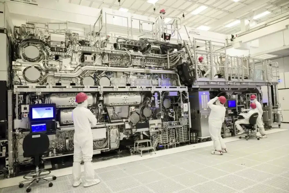
Intel has installed the world’s first commercial High-NA EUV lithography machine, ASML’s TWINSCAN EXE:5200B, marking a major milestone for advanced chip manufacturing. The system will be used to develop Intel’s upcoming 14A process node, which is expected to enter volume production in 2027.
High-NA EUV represents the industry’s shift beyond traditional Low-NA EUV, enabling much finer patterning with fewer manufacturing steps. Intel says the technology can reduce certain critical layers from around 40 steps to fewer than 10, significantly shortening cycle times and improving efficiency.
The EXE:5200B delivers 175 wafers per hour, with Intel planning to tune throughput beyond 200 WPH, while achieving an industry-leading 0.7nm overlay accuracy. It also integrates a higher-power EUV light source and a redesigned wafer handling system to improve thermal stability, alignment, and long-run consistency.
Intel began working with High-NA EUV in 2023 using ASML’s first-generation EXE:5000 tool and reports that 14A development is progressing faster and with better yields than 18A at the same stage. The company has already started shipping 14A PDK 0.5 to customers.
While early capacity will be limited, Intel plans to expand its High-NA EUV fleet over time, running 18A and 14A in parallel. With this installation, Intel becomes the first chipmaker to move High-NA EUV from research into commercial production, a critical step in its effort to reclaim semiconductor manufacturing leadership.