In an advancement that could reshape the future of materials science and quantum computing, physicists have developed a new quantum sensor capable of detecting individual electrical charges with unprecedented precision at the atomic scale. This tool allows researchers to observe and track the behavior of single electrons in real time, revealing defects in materials that were previously invisible.
The research, led by Professor Dr. Tim Schröder at Humboldt-Universität zu Berlin and the Ferdinand-Braun-Institut, was recently published in the journal Nature Communications.
The Unseen Flaws in Perfect Crystals
Modern technology, from computer chips to quantum devices, relies on highly ordered solid-state materials like silicon. However, even the most perfect-looking crystals can have tiny irregularities in their atomic lattice, such as a single missing atom. These defects can trap individual electrons, creating localized electric charges that generate electromagnetic noise. This noise can interfere with the performance of quantum bits (qubits) and limit the efficiency of electronic components, but locating these infinitesimal charge traps has been an immense challenge.
Using One Defect to Find Another
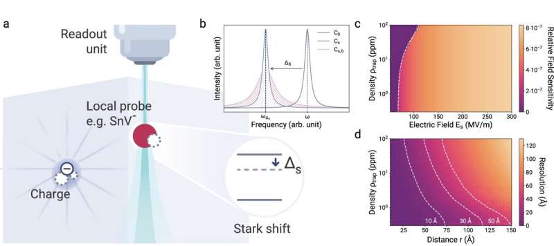
The research team’s innovative approach was to fight fire with fire—or rather, to use one crystal defect to detect another. They harnessed a specific type of defect, a color center, which is an imperfection in a synthetic diamond crystal that can absorb and emit light.
This color center is exceptionally sensitive to electric fields. The researchers embedded it into a tiny, rectangular piece of artificial diamond, creating the core of their sensor. When a single electric charge is trapped nearby, it slightly alters the electric field, which in turn causes a measurable change in the color of the light emitted by the color center.
“If a single charge is captured near the sensor, the color changes are clearly visible,” explains Dr. Gregor Pieplow, who developed the software for the sensor. “But if the charges are only a little further away, they cause almost no changes. This enables extremely precise determination of individual defects.”
Real-Time Observation at the Atomic Scale
A key feature of this new method is its speed. The sensor can take measurements at intervals of up to one-millionth of a second, allowing scientists to monitor the movement and behavior of charges in real time. This provides a dynamic view of physical processes that were once static or entirely hidden.
“This device is a new tool for researchers in materials science,” says Dr. Pieplow. “It makes physical processes, which we were previously unable to observe, visible and helps us understand them.”
Future Applications and Potential
The potential applications for this sensor extend far beyond its initial demonstration. The team has already filed for patents in Germany and the U.S. for the method and device.
“The integration of color centers into microscopic diamond tips will make it possible to analyze a wide variety of materials and realize a truly atomic, time-resolved, and fast scanning sensor,” adds Cem Güney Torun, who worked on the experimental design.
This capability could accelerate the development of new materials for:
- Next-Generation Quantum Computers: By identifying and mitigating charge noise that disrupts qubits.
- Advanced Semiconductors: By allowing engineers to pinpoint atomic-scale flaws that limit performance.
- Fundamental Materials Science: By providing a window into the behavior of electrons and defects in a wide range of quantum materials.
This new quantum sensor effectively provides atomic-scale MRI, offering a powerful new lens through which to view and engineer the materials that will define the future of technology.