A recently surfaced patent application from AMD has sparked excitement in the tech world, outlining a novel memory module design that could potentially double the effective bandwidth of standard DDR5 memory. Dubbed the “High-Bandwidth Dual Inline Memory Module” (HB-DIMM), the technology aims to address the growing bottleneck between modern processors and memory speeds.
Clever Engineering, Not New Chips
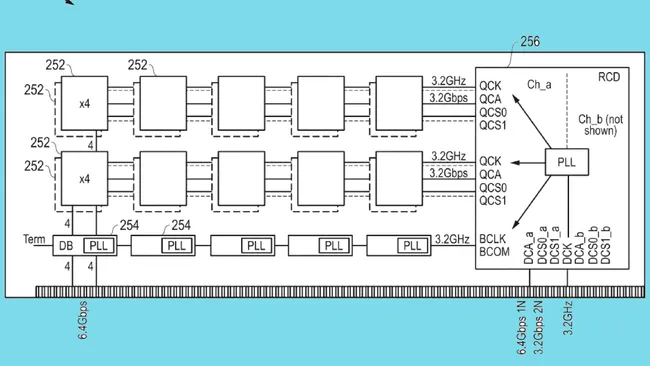
The core innovation of HB-DIMM lies not in creating new, faster memory chips, but in using existing DDR5 chips more intelligently. The design incorporates:
- Buffer Chips: Acting as high-speed intermediaries between the memory chips and the CPU.
- Pseudo-Channels: Splitting a single physical memory module into two independently addressable logical channels.
- Intelligent Signaling: Using an advanced Register Clock Driver (RCD) to manage data routing.
The net result is a design that can take standard DDR5 chips with a native speed of 6.4 Gbps and deliver an effective data rate of 12.8 Gbps to the host system, effectively doubling the bandwidth without requiring a new generation of DRAM silicon.
The Adoption Hurdle
However, the path from patent to product is fraught with challenges. For HB-DIMM to succeed, it requires support from CPU manufacturers (including Intel), motherboard manufacturers, and the broader industry. Proprietary memory standards have a poor track record in the PC market, which thrives on universal JEDEC standards. The biggest question is whether this technology will remain exclusive to AMD or be adopted by the industry standards body, JEDEC, to become a universal feature.
Why This Patent Isn’t What It Seems
The Truth Behind AMD’s Memory Patent: It’s Already Obsolete, and Here’s What We’re Getting Instead
While AMD’s “HB-DIMM” patent generated buzz, a closer look reveals it’s not a glimpse into the future, but rather a look into the past. The recently highlighted filing is a continuation of a 2022 patent, and the core technology it describes has already been superseded by an official industry standard that is already shipping in servers today.
From Competing Proposals to a Unified Standard
Around the same time AMD was developing its HB-DIMM concept, Intel and SK Hynix were working on a similar technology called MCR-DIMM. To avoid a costly format war with two incompatible standards, the industry giants took their proposals to JEDEC. The result is MRDIMM (Multiplexed Rank DIMM), a standardized technology that consolidates the best ideas from both HB-DIMM and MCR-DIMM.
MRDIMM is Here Now
This is not a future technology. MRDIMMs are already on the market and are supported by Intel’s current Xeon 6 server processors. Early benchmarks demonstrate notable performance gains in memory-intensive workloads, such as scientific computing, confirming the concept’s real-world value.
AMD’s Real Plans: Embracing the Standard
So, what is AMD’s plan? The evidence suggests the company has fully embraced the JEDEC standard. AMD’s next-generation EPYC “Venice” server CPUs, based on the Zen 6 architecture, are widely expected to support second-generation MRDIMMs. This aligns perfectly with CEO Dr. Lisa Su’s teaser of achieving 1.6 TB/s of per-socket memory bandwidth, a figure that matches the projected speed of these advanced memory modules.
The Bottom Line for Consumers and Businesses
The key takeaway is that the high-bandwidth memory future is already taking shape in the data center. For consumer PCs, the technology may trickle down eventually, but the high cost of MRDIMMs (currently 28% to 114% more expensive than standard DDR5) will keep it in the server realm for the foreseeable future. The AMD patent was a stepping stone to the real innovation: a standardized, collaborative solution that is already pushing the boundaries of server performance.