Intel Foundry Unveils Breakthroughs in Interconnect Scaling for Future Nodes

At IEDM 2024, Intel Foundry’s Technology Research team demonstrated industry-first advancements in transistor and packaging technologies that help meet future demands for AI.

At the IEEE International Electron Devices Meeting (IEDM) 2024, Intel Foundry unveiled breakthroughs to help drive the semiconductor industry forward into the next decade. Intel Foundry showcased new material advancements that help improve interconnections within a chip, resulting in up to 25% capacitance using subtractive ruthenium. Intel Foundry was also the first to report a 100x throughput improvement using a heterogeneous integration solution for advanced packaging to enable ultra-fast chip-to-chip assembly. To further drive gate-all-around (GAA) scaling, Intel Foundry demonstrated work with silicon RibbonFET CMOS and gate oxide module for scaled 2D FETs for improved device performance.

“Intel Foundry continues to help define and shape the roadmap for the semiconductor industry. Our latest breakthroughs underscore the company’s commitment to delivering cutting-edge technology developed in the U.S., positioning us well to help balance the global supply chain and restore domestic manufacturing and technology leadership with the support of the U.S. CHIPS Act.”

–Sanjay Natarajan, Intel senior vice president and general manager of Intel Foundry Technology Research
Why It Matters: As the industry heads toward putting 1 trillion transistors on a chip by 2030, breakthroughs in transistor and interconnect scaling—multiplied by future advanced packaging capabilities—are critical for satisfying the endless appetite for more energy-efficient, high-performing, and cost-effective computing applications such as AI.

The industry will also require additional support in the form of new materials to augment Intel Foundry’s PowerVia backside power delivery, relieving interconnect crowding and enabling continued scaling. This is vital to the continuation of Moore’s Law and driving the semiconductor forward into new eras for AI.

How We are Doing It:  Intel Foundry has identified several paths that solve anticipated limitations of copper transistors in interconnect scaling for future nodes, improve upon existing assembly techniques, and continue to define and shape the transistor roadmap for gate-all-around scaling and beyond:

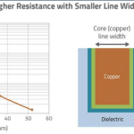
  • Subtractive Ruthenium (Ru): To help improve the performance and interconnections within chips, Intel Foundry showcased subtractive ruthenium, a new key alternative metallization material that uses thin film resistivity along with airgaps to deliver a significant advancement in interconnect scaling. The team was first to demonstrate, in R&D test vehicles, a practical, cost-efficient, and high-volume manufacturing compatible subtractive Ru integrated process with airgaps that does not require expensive lithographic airgap exclusion zones around vias or self-aligned via flows that require selective etches. The implementation of airgaps with subtractive Ru provided up to 25% of line-to-line capacitance reduction at pitches less than or equal to 25 nanometers (nm), illustrating the benefits of subtractive Ru as a metallization scheme to replace copper damascene in tight pitch layers. This solution could be seen on Intel Foundry’s future nodes.
  • Selective Layer Transfer (SLT): To enable up to 100x higher throughput for ultra-fast chip-to-chip assembly in advanced packaging, Intel Foundry is the first to demonstrate Selective Layer Transfer (SLT). This heterogeneous integration solution enables ultra-thin chiplets with much better flexibility, enabling smaller die sizes and higher aspect ratios versus traditional chip-to-wafer bonding. This allows higher functional density and leads to a more flexible and cost-efficient solution for hybrid or fusion bonding of specific chiplets from one wafer to another. This solution offers a more efficient and flexible architecture for AI applications.
  • Silicon RibbonFET CMOS: To push gate-all-around RibbonFET silicon scaling to its limits, Intel Foundry showcased silicon RibbonFET CMOS (complementary metal oxide semiconductor) transistors at a gate length of 6 nm with industry-leading short channel effects and performance at aggressively scaled gate length and channel thickness. This advancement paves the way for continued gate length scaling, one of the key foundational cornerstones of Moore’s Law.
  • Gate Oxide for Scaled GAA 2D FETs: To further accelerate gate-all-around innovation beyond CFET, Intel Foundry showcased its work on the fabrication of GAA 2D NMOS and PMOS transistors with scaled gate length down to 30 nm with a specific focus on gate oxide (GOx) module development. The research reports on the industry’s investigation of two-dimensional (2D) transition metal dichalcogenide (TMD) semiconductors, which may be a future replacement for silicon in advanced transistor processes.

Additionally, Intel Foundry continued to advance research with the industry’s first 300 millimeter (mm) gallium nitride (GaN) technology, an emerging technology for power and radio frequency (RF) electronics that can deliver higher performance and sustain higher voltages and temperatures than silicon. This is the industry’s first high-performance scaled enhancement-mode GaN MOSHEMTs (metal-oxide-semiconductor high electron mobility transistors), fabricated on a 300 mm GaN-on-TRSOI (“trap-rich” silicon-on-insulator) substrate. Advanced-engineered substrates like GaN-on-TRSOI can achieve better performance in applications such as RF and power electronics by reducing signal loss and improving signal linearity, enabling advanced integration schemes that may be realized through backside substrate processing.

Related Posts

Leave a Reply

Your email address will not be published. Required fields are marked *